恭喜您提交成功
 提交失敗
提交失敗
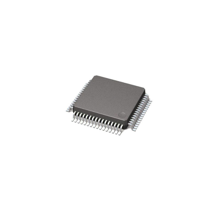
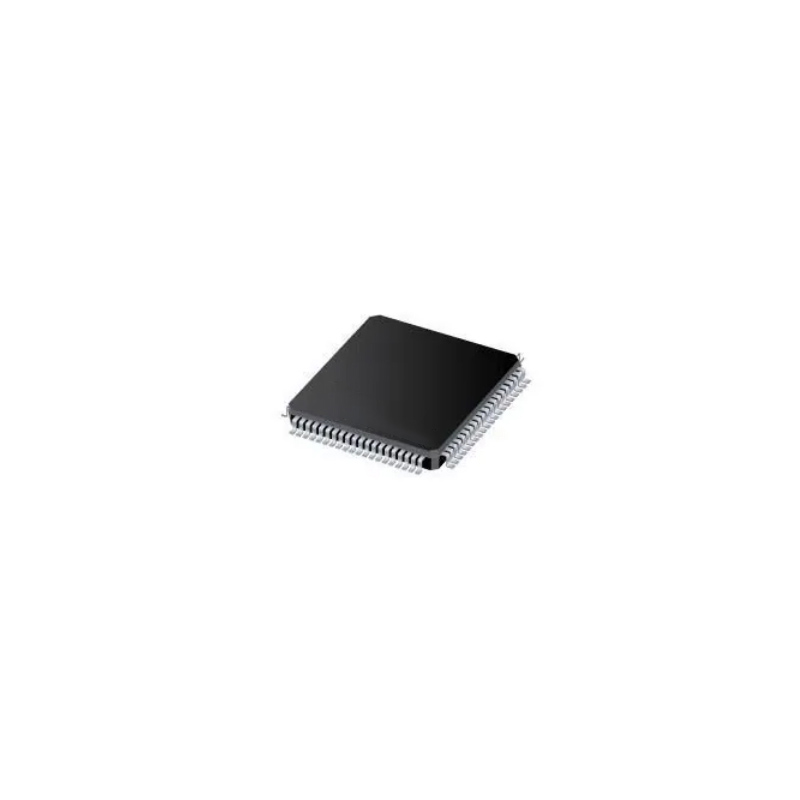
XPC860TZP50D4
High-performance communications controller suitable for advanced networking applications
XPC860TZP50D4
High-performance communications controller suitable for advanced networking applications
-
製造商零件號 # : XPC860TZP50D4
-
包裝/封裝: BGA
-
製造商: FREESCALE
-
產品分類 : Microprocessors
品質保證
品質保證
從我們的供應鍊網路採購的所有零件都經過嚴格的進貨檢驗流程。 這種細緻的檢查可確保客戶收到的零件是正品並符合要求的標準。 此外,我們還保存這些檢查的詳細記錄,以確保整個供應鏈的透明度和可追溯性。


認證
我們已成功獲得各項認證標準,並建立了自己的專業檢測實驗室。 這確保了我們向客戶提供的每件產品都符合最高的品質標準。 我們遵守嚴格的測試協議,以保持我們產品的一致性和準確性。 為了確保我們的產品是原裝正品,我們還與信譽良好的第三方檢測機構合作進行嚴格的品質測試。 我們對品質的承諾延伸到滿足行業、法律、監管和 ISO 9001:2015 的要求。
運輸與付款
運輸與付款
關於運送
我們通常會在幾個工作日內通過可靠的運輸公司(例如 FedEx、SF、UPS 或 DHL)運送訂單。 我們還支持其他運輸方式。 如果您想詢問具體的運輸細節或費用,請隨時與我們聯繫。


關於付款
我們接受多種支付方式,包括VISA、MasterCard、銀聯、西聯、PayPal等渠道。
如果您有特定的付款方式或想詢問費率和其他詳細信息,請隨時與我們聯繫。

電匯

Paypal

信用卡

西聯匯款

速匯金
服務與包裝
服務與包裝
About After Sales Service
All Parts Extended Quality Guarantee
自發貨之日起 90 天內發起申請。
與我們的工作人員確認退貨或換貨。
保持貨物收到時的原始狀態。
最後請注意,退貨或換貨的資格取決於對退貨商品實際狀況的評估。 在完成退貨或換貨流程之前,我們將評估收到的貨物。 如果您對退貨或換貨有任何疑問或需要進一步幫助,請隨時通過以下方式聯絡我們: [email protected]
關於包裝
在包裝方面,我們的產品均精心包裝在防靜電袋中,以提供ESD防靜電保護。 外包裝堅固耐用且閉合牢固。 我們支持各種包裝方法,例如捲帶式、切帶式、管式或託盤式。

例子

捲帶式

剪膠帶

管或託盤
XPC860TZP50D4 數據表

目前的價格方案正在編制中。請聯絡我們的客戶服務團隊獲取最新的價格資訊。感謝您的理解和支援!
詳細說明
Overview The MPC860 Quad Integrated Communications Controller (PowerQUICC™) is a versatile one-chip integrated microprocessor and peripheral combination designed for a variety of controller applications. It particularly excels in both communications and networking systems. The PowerQUICC unit is referred to as the MPC860 in this manual.Features The following list summarizes the key MPC860 features: • Embedded single-issue, 32-bit MPC8xx core (implementing the PowerPC architecture) with thirty-two 32-bit general-purpose registers (GPRs) — The core performs branch prediction with conditional prefetch, without conditional execution — 4- or 8-Kbyte data cache and 4- or 16-Kbyte instruction cache (see Table 1) – 16-Kbyte instruction caches are four-way, set-associative with 256 sets; 4-Kbyte instruction caches are two-way, set-associative with 128 sets. – 8-Kbyte data caches are two-way, set-associative with 256 sets; 4-Kbyte data caches are two-way, set-associative with 128 sets. – Cache coherency for both instruction and data caches is maintained on 128-bit (4-word) cache blocks. – Caches are physically addressed, implement a least recently used (LRU) replacement algorithm, and are lockable on a cache block basis. — Instruction and data caches are two-way, set-associative, physically addressed, LRU replacement, and lockable on-line granularity. — MMUs with 32-entry TLB, fully associative instruction, and data TLBs — MMUs support multiple page sizes of 4, 16, and 512 Kbytes, and 8 Mbytes; 16 virtual address spaces and 16 protection groups — Advanced on-chip-emulation debug mode • Up to 32-bit data bus (dynamic bus sizing for 8, 16, and 32 bits) • 32 address lines • Operates at up to 80 MHz • Memory controller (eight banks) — Contains complete dynamic RAM (DRAM) controller — Each bank can be a chip select or RASto support a DRAM bank — Up to 15 wait states programmable per memory bank — Glueless interface to DRAM, SIMMS, SRAM, EPROM, Flash EPROM, and other memory devices. — DRAM controller programmable to support most size and speed memory interfaces — Four CASlines, four WElines, one OEline — Boot chip-select available at reset (options for 8-, 16-, or 32-bit memory) — Variable block sizes (32 Kbyte to 256 Mbyte) — Selectable write protection — On-chip bus arbitration logic • General-purpose timers — Four 16-bit timers or two 32-bit timers — Gate mode can enable/disable counting — Interrupt can be masked on reference match and event capture • System integration unit (SIU) — Bus monitor — Software watchdog — Periodic interrupt timer (PIT) — Low-power stop mode — Clock synthesizer — Three parallel I/O registers with open-drain capability • Four baud-rate generators (BRGs) — Independent (can be connected to any SCC or SMC) — Allow changes during operation — Autobaud support option • Four serial communications controllers (SCCs) — Ethernet/IEEE 802.3 optional on SCC1–4, supporting full 10-Mbps operation (available only on specially programmed devices). — HDLC/SDLC(all channels supported at 2 Mbps) — HDLC bus (implements an HDLC-based local area network (LAN)) — Asynchronous HDLC to support PPP (point-to-point protocol) — AppleTalk — Universal asynchronous receiver transmitter (UART) — Synchronous UART — Serial infrared (IrDA) — Binary synchronous communication (BISYNC) — Totally transparent (bit streams) — Totally transparent (frame based with optional cyclic redundancy check (CRC)) • Two SMCs (serial management channels) — UART — Transparent — General circuit interface (GCI) controller — Can be connected to the time-division multiplexed (TDM) channels • One SPI (serial peripheral interface) — Supports master and slave modes — Supports multimaster operation on the same bus • One I2C (inter-integrated circuit) port — Supports master and slave modes — Multiple-master environment support • Time-slot assigner (TSA) — Allows SCCs and SMCs to run in multiplexed and/or non-multiplexed operation — Supports T1, CEPT, PCM highway, ISDN basic rate, ISDN primary rate, user defined — 1- or 8-bit resolution — Allows independent transmit and receive routing, frame synchronization, clocking — Allows dynamic changes — Can be internally connected to six serial channels (four SCCs and two SMCs) • Parallel interface port (PIP) — Centronics interface support — Supports fast connection between compatible ports on the MPC860 or the MC68360 • PCMCIA interface — Master (socket) interface, release 2.1 compliant — Supports two independent PCMCIA sockets — Eight memory or I/O windows supported • Low power support — Full on—all units fully powered — Doze—core functional units disabled, except time base decrementer, PLL, memory controller, RTC, and CPM in low-power standby — Sleep—all units disabled, except RTC and PIT, PLL active for fast wake up — Deep sleep—all units disabled including PLL, except RTC and PIT — Power down mode— all units powered down, except PLL, RTC, PIT, time base, and decrementer • Debug interface — Eight comparators: four operate on instruction address, two operate on data address, and two operate on data — Supports conditions: =≠<> — Each watchpoint can generate a break-point internally • 3.3 V operation with 5-V TTL compatibility except EXTAL and EXTCLK • 357-pin ball grid array (BGA) package
主要特徵
- The following list summarizes the key MPC860
- features:
- Embedded single-issue, 32-bit MPC8xx core (implementing the PowerPC architecture) with thirty-two 32-bit general-purpose registers (GPRs)
- — The core performs branch prediction with conditional prefetch, without conditional execution
- — 4- or 8-Kbyte data cache and 4- or 16-Kbyte instruction cache (see Table 1)
- – 16-Kbyte instruction caches are four-way, set-associative with 256 sets;
- 4-Kbyte instruction caches are two-way, set-associative with 128 sets.
- – 8-Kbyte data caches are two-way, set-associative with 256 sets; 4-Kbyte data caches are two-way, set-associative with 128 sets.
- – Cache coherency for both instruction and data caches is maintained on 128-bit (4-word) cache blocks.
- – Caches are physically addressed, implement a least recently used (LRU) replacement algorithm, and are lockable on a cache block basis.
- — Instruction and data caches are two-way, set-associative, physically addressed, LRU replacement, and lockable on-line granularity.
- — MMUs with 32-entry TLB, fully associative instruction, and data TLBs
- — MMUs support multiple page sizes of 4, 16, and 512 Kbytes, and 8 Mbytes; 16 virtual address spaces and 16 protection groups
- — Advanced on-chip-emulation debug mode
- Up to 32-bit data bus (dynamic bus sizing for 8, 16, and 32 bits)
- 32 address lines
- Operates at up to 80 MHz
- Memory controller (eight banks)
- — Contains complete dynamic RAM (DRAM) controller
- — Each bank can be a chip select or RASto support a DRAM bank
- — Up to 15 wait states programmable per memory bank
- — Glueless interface to DRAM, SIMMS, SRAM, EPROM, Flash EPROM, and other memory devices.
- — DRAM controller programmable to support most size and speed memory interfaces
- — Four CASlines, four WElines, one OEline
- — Boot chip-select available at reset (options for 8-, 16-, or 32-bit memory)
- — Variable block sizes (32 Kbyte to 256 Mbyte)
- — Selectable write protection
- — On-chip bus arbitration logic
- General-purpose timers
- — Four 16-bit timers or two 32-bit timers
- — Gate mode can enable/disable counting
- — Interrupt can be masked on reference match and event capture
- System integration unit (SIU)
- — Bus monitor
- — Software watchdog
- — Periodic interrupt timer (PIT)
- — Low-power stop mode
- — Clock synthesizer
- — Three parallel I/O registers with open-drain capability
- Four baud-rate generators (BRGs)
- — Independent (can be connected to any SCC or SMC)
- — Allow changes during operation
- — Autobaud support option
- Four serial communications controllers (SCCs)
- — Ethernet/IEEE 802.3 optional on SCC1–4, supporting full 10-Mbps operation (available only on specially programmed devices).
- — HDLC/SDLC(all channels supported at 2 Mbps)
- — HDLC bus (implements an HDLC-based local area network (LAN))
- — Asynchronous HDLC to support PPP (point-to-point protocol)
- — AppleTalk
- — Universal asynchronous receiver transmitter (UART)
- — Synchronous UART
- — Serial infrared (IrDA)
- — Binary synchronous communication (BISYNC)
- — Totally transparent (bit streams)
- — Totally transparent (frame based with optional cyclic redundancy check (CRC))
- Two SMCs (serial management channels)
- — UART
- — Transparent
- — General circuit interface (GCI) controller
- — Can be connected to the time-division multiplexed (TDM) channels
- One SPI (serial peripheral interface)
- — Supports master and slave modes
- — Supports multimaster operation on the same bus
- One I2C (inter-integrated circuit) port
- — Supports master and slave modes
- — Multiple-master environment support
- Time-slot assigner (TSA)
- — Allows SCCs and SMCs to run in multiplexed and/or non-multiplexed operation
- — Supports T1, CEPT, PCM highway, ISDN basic rate, ISDN primary rate, user defined
- — 1- or 8-bit resolution
- — Allows independent transmit and receive routing, frame synchronization, clocking
- — Allows dynamic changes
- — Can be internally connected to six serial channels (four SCCs and two SMCs)
- Parallel interface port (PIP)
- — Centronics interface support
- — Supports fast connection between compatible ports on the MPC860 or the MC68360
- PCMCIA interface
- — Master (socket) interface, release 2.1 compliant
- — Supports two independent PCMCIA sockets
- — Eight memory or I/O windows supported
- Low power support
- — Full on—all units fully powered
- — Doze—core functional units disabled, except time base decrementer, PLL, memory controller, RTC, and CPM in low-power standby
- — Sleep—all units disabled, except RTC and PIT, PLL active for fast wake up
- — Deep sleep—all units disabled including PLL, except RTC and PIT
- — Power down mode— all units powered down, except PLL, RTC, PIT, time base, and decrementer
- Debug interface
- — Eight comparators: four operate on instruction address, two operate on data address, and two operate on data
- — Supports conditions: =≠<>
- — Each watchpoint can generate a break-point internally
- 3.3 V operation with 5-V TTL compatibility except EXTAL and EXTCLK
- 357-pin ball grid array (BGA) package
規格
以下是所選零件的基本參數,涉及零件的特性及其所屬類別。
| Rohs Code | No | Part Life Cycle Code | Obsolete |
| Part Package Code | BGA | Pin Count ! | 357 |
| Reach Compliance Code | not_compliant | ECCN Code | 5A991 |
| HTS Code ! | 8542.31.00.01 | Address Bus Width ! | 32 |
| Bit Size | 32 | Boundary Scan | YES |
| Clock Frequency-Max | 50 MHz | External Data Bus Width | 32 |
| Format | FIXED POINT | Integrated Cache | YES |
| JESD-30 Code | S-PBGA-B357 | JESD-609 Code | e0 |
| Length | 25 mm | Low Power Mode | YES |
| Moisture Sensitivity Level | 3 | Number of Terminals | 357 |
| Operating Temperature-Min | Package Body Material | PLASTIC/EPOXY | |
| Package Code | BGA | Package Equivalence Code | BGA357,19X19,50 |
| Package Shape | SQUARE | Package Style | GRID ARRAY |
| Peak Reflow Temperature (Cel) | 220 | Power Supplies ! | 3.3 V |
| Qualification Status ! | Not Qualified | Seated Height-Max | 2.05 mm |
| Speed | 50 MHz | Supply Voltage-Max | 3.465 V |
| Supply Voltage-Min | 3.135 V | Supply Voltage-Nom | 3.3 V |
| Surface Mount ! | YES | Technology | CMOS |
| Terminal Finish | Tin/Lead/Silver (Sn/Pb/Ag) | Terminal Form ! | BALL |
| Terminal Pitch ! | 1.27 mm | Terminal Position | BOTTOM |
| Time@Peak Reflow Temperature-Max (s) | 30 | Width | 25 mm |
| uPs/uCs/Peripheral ICs Type | MICROPROCESSOR, RISC |
數據表 PDF
數據表記錄了器件的特性、絕對最大額定值、應用等,這對於作為器件特定應用的整體指南大有裨益。
推薦零件
-
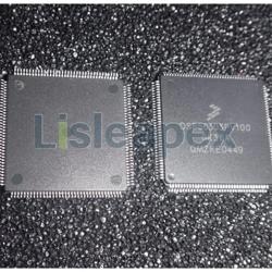
![DSP56303PV100]()
DSP56303PV100 offers high-speed processing capabilities with 24-bit fixed-point precision
製造商: Nxp Semiconductors 包裝/箱: LQFP-144
3,456 有存貨
貨物週期: 3~7 天
最小訂購量為 1
-
![MC68331CFC20]()
This microcontroller operates on a High-Speed CMOS technology, housed in a PQFP132 package made of plastic
製造商: FREESCALE 包裝/箱: QFP132
6,374 有存貨
貨物週期: 3~7 天
最小訂購量為 1
-
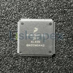
![MC9S12DT128]()
The MC9S12DT128 is a 16-bit microcontroller chip by Freescale (now NXP)
製造商: FREESCALE 包裝/箱: TQFP11
7,695 有存貨
貨物週期: 3~7 天
最小訂購量為 1
-
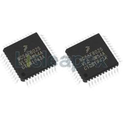
![MC56F8025V]()
7,729 有存貨
貨物週期: 3~7 天
最小訂購量為 1
-
![MC9S08GB60A]()
3,328 有存貨
貨物週期: 3~7 天
最小訂購量為 1
-
![MC68HC912D60A]()
MC68HC912D60A is a 16-bit microcontroller from Freescale, suitable for automotive and industrial applications.
製造商: FREESCALE 包裝/箱: QFP
1 有存貨
貨物週期: 3~7 天
最小訂購量為 1
-
![MC68HC912D60]()
MC68HC912D60 is a 16-bit microcontroller chip with 60KB flash memory and 2KB RAM for embedded systems.
製造商: FREESCALE 包裝/箱: QFP
3,454 有存貨
貨物週期: 3~7 天
最小訂購量為 1