恭喜您提交成功
 提交失敗
提交失敗

LX64V-3F100C
IC FPGA 64 I/O 100FPBGA
-
製造商零件號 # : LX64V-3F100C
-
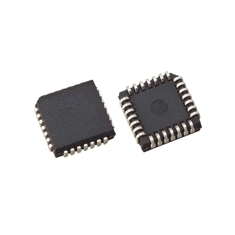
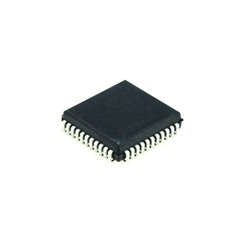
包裝/封裝: FPBGA-100
-
零件狀態 : Obsolete
品質保證
品質保證
從我們的供應鍊網路採購的所有零件都經過嚴格的進貨檢驗流程。 這種細緻的檢查可確保客戶收到的零件是正品並符合要求的標準。 此外,我們還保存這些檢查的詳細記錄,以確保整個供應鏈的透明度和可追溯性。


認證
我們已成功獲得各項認證標準,並建立了自己的專業檢測實驗室。 這確保了我們向客戶提供的每件產品都符合最高的品質標準。 我們遵守嚴格的測試協議,以保持我們產品的一致性和準確性。 為了確保我們的產品是原裝正品,我們還與信譽良好的第三方檢測機構合作進行嚴格的品質測試。 我們對品質的承諾延伸到滿足行業、法律、監管和 ISO 9001:2015 的要求。
運輸與付款
運輸與付款
關於運送
我們通常會在幾個工作日內通過可靠的運輸公司(例如 FedEx、SF、UPS 或 DHL)運送訂單。 我們還支持其他運輸方式。 如果您想詢問具體的運輸細節或費用,請隨時與我們聯繫。


關於付款
我們接受多種支付方式,包括VISA、MasterCard、銀聯、西聯、PayPal等渠道。
如果您有特定的付款方式或想詢問費率和其他詳細信息,請隨時與我們聯繫。

電匯

Paypal

信用卡

西聯匯款

速匯金
服務與包裝
服務與包裝
About After Sales Service
All Parts Extended Quality Guarantee
自發貨之日起 90 天內發起申請。
與我們的工作人員確認退貨或換貨。
保持貨物收到時的原始狀態。
最後請注意,退貨或換貨的資格取決於對退貨商品實際狀況的評估。 在完成退貨或換貨流程之前,我們將評估收到的貨物。 如果您對退貨或換貨有任何疑問或需要進一步幫助,請隨時通過以下方式聯絡我們: [email protected]
關於包裝
在包裝方面,我們的產品均精心包裝在防靜電袋中,以提供ESD防靜電保護。 外包裝堅固耐用且閉合牢固。 我們支持各種包裝方法,例如捲帶式、切帶式、管式或託盤式。

例子

捲帶式

剪膠帶

管或託盤
LX64V-3F100C 數據表

目前的價格方案正在編制中。請聯絡我們的客戶服務團隊獲取最新的價格資訊。感謝您的理解和支援!
詳細說明
The LX64V-3F100C is a highly configurable digital crosspoint switch from Lattice Semiconductor Corporation, designed for various communication and networking applications. This IC FPGA features 64 I/Os and operates at 11 Gb/s, making it suitable for high-speed data transmission and switching needs. The device can be configured as a 64 x 64 crossbar, allowing for flexible routing of signals between inputs and outputs. The LX64V-3F100C is packaged in a 100-LBGA (Lead-Frame Bump Grid Array) and is powered by a triple supply voltage scheme.
主要特徵
- Configurable 64 x 64 digital crosspoint switch
- Operates at speeds of up to 11 Gb/s
- Supports multiple input and output types, including LVDS, LVCMOS, LVPECL, and LVTTL
- Triple supply voltage configuration (3.3 V, 3.0 V, and 2.5 V)
- Operating temperature range: -40°C to +125°C (jammed), -10°C to +90°C (unjammed)
- SMD/SMT package type
應用
- High-speed data transmission and switching in communication networks
- Flexible routing of signals between inputs and outputs in various applications
- Switching and multiplexing in digital signal processing systems
- Configuration control and management in distributed systems
規格
以下是所選零件的基本參數,涉及零件的特性及其所屬類別。
| Product Category ! | Analog & Digital Crosspoint ICs | RoHS | N |
| Product | Digital Crosspoint Switches | Configuration | 64 x 64 |
| Data Rate ! | 11 Gb/s | Input Type | Bus LVDS, LVCMOS, LVDS, LVPECL, LVTTL |
| Output Type | Bus LVDS, LVCMOS, LVDS, LVPECL, LVTTL | Operating Supply Voltage ! | 3.3 V |
| Minimum Operating Temperature | 0 C | Maximum Operating Temperature ! | + 90 C |
| Mounting Style | SMD/SMT | Package / Case | FPBGA-100 |
| Brand | Lattice | Height | 1.1 mm |
| Length | 11 mm | Maximum Dual Supply Voltage | 3.6 V |
| Minimum Dual Supply Voltage | 3 V | Moisture Sensitive | Yes |
| Product Type ! | Analog & Digital Crosspoint ICs | Factory Pack Quantity | 1 |
| Subcategory | Communication & Networking ICs | Supply Type | Triple |
| Width | 11 mm |
常見問題解答
What is LX64V-3F100C?
The LX64V-3F100C is a low-cost, high-performance field-programmable gate array (FPGA) developed by Lattice Semiconductor. It is designed for applications that require high logic density, low power consumption, and fast time-to-market, such as industrial automation, communication infrastructure, and consumer electronics.
How Does LX64V-3F100C Work?
The LX64V-3F100C works by providing a reconfigurable platform for implementing digital logic functions. It consists of configurable logic blocks (CLBs), dedicated input/output blocks, and embedded memory to support a wide range of digital designs. The FPGA can be programmed and reprogrammed to perform specific tasks, allowing flexibility in system development.
How Many Pins does LX64V-3F100C have and What are the Functions of the Pinout Configuration?
The LX64V-3F100C is housed in a 100-pin TQFP (Thin Quad Flat Package) package. The pinout configuration includes:
- IOBs: Input/output blocks for interfacing with external components.
- CLBs: Configurable logic blocks for implementing logic functions.
- Global Clock Networks and Buffers: Provide clock distribution and conditioning for internal and external clock signals.
- Configuration Pins: Pins for configuring the FPGA and managing startup operations.
- Power and Ground Pins: Provide power supply and ground connections for the device.
What are the Pros and Cons of LX64V-3F100C?
Pros:
- High Logic Density: Offers a large number of configurable logic blocks for complex designs.
- Low Power Consumption: Provides efficient power usage, suitable for battery-powered devices.
- Reconfigurability: Can be reprogrammed for different functions, allowing for design flexibility and upgrades.
- Integrated Memory: Includes embedded memory blocks for data storage and processing.
- Cost-Effective Solution: Provides a balance between performance and cost for various applications.
Cons:
- Complex Design Process: Designing with FPGAs may require specialized expertise and tools, adding complexity to development.
- Static Power Consumption: While low, FPGAs have static power consumption even when idle.
- I/O Limitations: The number of available input/output pins may limit connectivity in some applications.
Are There Any Equivalents/Alternatives to LX64V-3F100C for Recommendation?
- The ECP5-12F from Lattice Semiconductor is a similar low-cost FPGA with enhanced features.
- Alternatives to the LX64V-3F100C include the Spartan-7 series from Xilinx and the MachXO2 series from Lattice Semiconductor.
推薦零件
-
![ISPGDX160A-5Q208]()
Analog & Digital Crosspoint ICs PROGRAMMABLE GEN DIG CROSSPOINT
製造商: Lattice 包裝/箱: DIP-24
5,009 有存貨
貨物週期: 3~7 天
最小訂購量為 1
-
![GAL16V8D-15]()
GAL16V8D-15 is a high-performance, low-power programmable logic device with 15ns speed.
製造商: LATTICE 包裝/箱: SOP-20
5,097 有存貨
貨物週期: 3~7 天
最小訂購量為 1
-
![GAL16V8C-5LJ]()
7,287 有存貨
貨物週期: 3~7 天
最小訂購量為 1
-
![PALCE16V8Q]()
PALCE16V8Q is a Programmable Array Logic chip with 16 inputs and 8 outputs, suitable for logic functions.
製造商: LATTICE 包裝/箱: PLCC20
3,669 有存貨
貨物週期: 3~7 天
最小訂購量為 1
-
![PALCE22V10Q]()
PALCE22V10Q is a user-programmable logic device with 22 input/outputs and 10 macrocells.
製造商: LATTICE 包裝/箱: PLCC28
6,835 有存貨
貨物週期: 3~7 天
最小訂購量為 1
-
![PALCE16V8Z]()
PALCE16V8Z is a versatile SPLD chip with 16 inputs, 8 outputs, and 8 macrocells for logic functions.
製造商: LATTICE 包裝/箱: PLCC20
6,905 有存貨
貨物週期: 3~7 天
最小訂購量為 1
-
![PALCE20V8H]()
PALCE20V8H is a high-performance programmable logic device with 20 macrocells.
製造商: LATTICE 包裝/箱: PLCC28
6,132 有存貨
貨物週期: 3~7 天
最小訂購量為 1
-
![PALCE22V10H]()
PALCE22V10H is a low-power CMOS programmable logic device with 10 macrocells, optimized for high-performance applications.
製造商: LATTICE 包裝/箱: PLCC28
4,469 有存貨
貨物週期: 3~7 天
最小訂購量為 1
-
![PALCE22V10Z]()
PALCE22V10Z is a programmable logic device with 24 macrocells and 10 input pins.
製造商: LATTICE 包裝/箱: PLCC28
3,193 有存貨
貨物週期: 3~7 天
最小訂購量為 1