恭喜您提交成功
 提交失敗
提交失敗
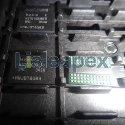
H5PS5162FFR-25C
CMOS DDR DRAM in PBGA84 package, HALOGEN FREE AND ROHS COMPLIANTH5PS5162FFR-25C
CMOS DDR DRAM in PBGA84 package, HALOGEN FREE AND ROHS COMPLIANT
-
製造商零件號 # : H5PS5162FFR-25C
-
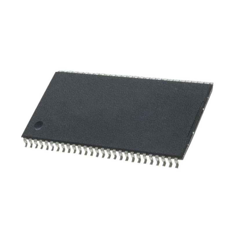
包裝/封裝: BGA84
-
製造商: SKHYNIX
-
產品分類 : Application Specific Clock/Timing
品質保證
品質保證
從我們的供應鍊網路採購的所有零件都經過嚴格的進貨檢驗流程。 這種細緻的檢查可確保客戶收到的零件是正品並符合要求的標準。 此外,我們還保存這些檢查的詳細記錄,以確保整個供應鏈的透明度和可追溯性。


認證
我們已成功獲得各項認證標準,並建立了自己的專業檢測實驗室。 這確保了我們向客戶提供的每件產品都符合最高的品質標準。 我們遵守嚴格的測試協議,以保持我們產品的一致性和準確性。 為了確保我們的產品是原裝正品,我們還與信譽良好的第三方檢測機構合作進行嚴格的品質測試。 我們對品質的承諾延伸到滿足行業、法律、監管和 ISO 9001:2015 的要求。
運輸與付款
運輸與付款
關於運送
我們通常會在幾個工作日內通過可靠的運輸公司(例如 FedEx、SF、UPS 或 DHL)運送訂單。 我們還支持其他運輸方式。 如果您想詢問具體的運輸細節或費用,請隨時與我們聯繫。


關於付款
我們接受多種支付方式,包括VISA、MasterCard、銀聯、西聯、PayPal等渠道。
如果您有特定的付款方式或想詢問費率和其他詳細信息,請隨時與我們聯繫。

電匯

Paypal

信用卡

西聯匯款

速匯金
服務與包裝
服務與包裝
About After Sales Service
All Parts Extended Quality Guarantee
自發貨之日起 90 天內發起申請。
與我們的工作人員確認退貨或換貨。
保持貨物收到時的原始狀態。
最後請注意,退貨或換貨的資格取決於對退貨商品實際狀況的評估。 在完成退貨或換貨流程之前,我們將評估收到的貨物。 如果您對退貨或換貨有任何疑問或需要進一步幫助,請隨時通過以下方式聯絡我們: [email protected]
關於包裝
在包裝方面,我們的產品均精心包裝在防靜電袋中,以提供ESD防靜電保護。 外包裝堅固耐用且閉合牢固。 我們支持各種包裝方法,例如捲帶式、切帶式、管式或託盤式。

例子

捲帶式

剪膠帶

管或託盤
H5PS5162FFR-25C 數據表

目前的價格方案正在編制中。請聯絡我們的客戶服務團隊獲取最新的價格資訊。感謝您的理解和支援!
詳細說明
Key Features• VDD = 1.8 +/- 0.1V• VDDQ = 1.8 +/- 0.1V• All inputs and outputs are compatible with SSTL_18 interface• 8 banks• Fully differential clock inputs (CK, /CK) operation• Double data rate interface• Source synchronous-data transaction aligned to bidirectional data strobe (DQS, DQS)• Differential Data Strobe (DQS, DQS)• Data outputs on DQS, DQS edges when read (edged DQ)• Data inputs on DQS centers when write (centered DQ)• On chip DLL align DQ, DQS and DQS transition with CK transition• DM mask write data-in at the both rising and falling edges of the data strobe• All addresses and control inputs except data, data strobes and data masks latched on the rising edges of the clock• Programmable CAS latency 3, 4, 5 and 6 supported• Programmable additive latency 0, 1, 2, 3, 4 and 5 supported• Programmable burst length 4/8 with both nibble sequential and interleave mode• Internal eight bank operations with single pulsed RAS• Auto refresh and self refresh supported• tRAS lockout supported• 8K refresh cycles /64ms• JEDEC standard 84ball FBGA(x16)• Full strength driver option controlled by EMR• On Die Termination supported• Off Chip Driver Impedance Adjustment supported• Self-Refresh High Temperature Entry• Average Refresh Cycle (Tcase 0 oC~ 95 oC) - 7.8 µs at 0oC ~ 85 oC - 3.9 µs at 85oC ~ 95 oC Commercial Temperature( 0oC ~ 85 oC) Industrial Temperature( -40oC ~ 95 oC)

主要特徵
- VDD = 1.8 +/- 0.1V
- VDDQ = 1.8 +/- 0.1V
- All inputs and outputs are compatible with SSTL_18 interface
- 8 banks
- Fully differential clock inputs (CK, /CK) operation
- Double data rate interface
- Source synchronous-data transaction aligned to bidirectional data strobe (DQS, DQS)
- Differential Data Strobe (DQS, DQS)
- Data outputs on DQS, DQS edges when read (edged DQ)
- Data inputs on DQS centers when write (centered DQ)
- On chip DLL align DQ, DQS and DQS transition with CK transition
- DM mask write data-in at the both rising and falling edges of the data strobe
- All addresses and control inputs except data, data strobes and data masks latched on the rising edges of the clock
- Programmable CAS latency 3, 4, 5 and 6 supported
- Programmable additive latency 0, 1, 2, 3, 4 and 5 supported
- Programmable burst length 4/8 with both nibble sequential and interleave mode
- Internal eight bank operations with single pulsed RAS
- Auto refresh and self refresh supported
- tRAS lockout supported
- 8K refresh cycles /64ms
- JEDEC standard 84ball FBGA(x16)
- Full strength driver option controlled by EMR
- On Die Termination supported
- Off Chip Driver Impedance Adjustment supported
- Self-Refresh High Temperature Entry
- Average Refresh Cycle (Tcase 0 oC~ 95 oC)
- - 7.8 µs at 0oC ~ 85 oC
- - 3.9 µs at 85oC ~ 95 oC
- Commercial Temperature( 0oC ~ 85 oC)
- Industrial Temperature( -40oC ~ 95 oC)
規格
以下是所選零件的基本參數,涉及零件的特性及其所屬類別。
| Rohs Code | Yes | Part Life Cycle Code | Obsolete |
| Part Package Code | BGA | Pin Count ! | 84 |
| Reach Compliance Code | ECCN Code | EAR99 | |
| HTS Code ! | 8542.32.00.28 | Access Mode ! | FOUR BANK PAGE BURST |
| Access Time-Max | 0.5 ns | Additional Feature ! | AUTO/SELF REFRESH |
| Clock Frequency-Max (fCLK) | 400 MHz | I/O Type | COMMON |
| Interleaved Burst Length | 4,8 | JESD-30 Code | R-PBGA-B208 |
| JESD-609 Code | e1 | Length | 13 mm |
| Memory Density | 536870912 bit | Memory IC Type | DDR2 DRAM |
| Memory Width | 16 | Number of Functions | 1 |
| Number of Ports ! | 1 | Number of Terminals | 84 |
| Number of Words | 33554432 words | Number of Words Code | 32000000 |
| Operating Mode ! | SYNCHRONOUS | Operating Temperature-Max | 85 °C |
| Operating Temperature-Min | Organization | 32MX16 | |
| Output Characteristics | 3-STATE | Package Body Material | PLASTIC/EPOXY |
| Package Code | TFBGA | Package Equivalence Code | BGA84,9X15,32 |
| Package Shape | RECTANGULAR | Package Style | GRID ARRAY |
| Peak Reflow Temperature (Cel) | 260 | Power Supplies ! | 1.8 V |
| Qualification Status ! | Not Qualified | Refresh Cycles | 8192 |
| Seated Height-Max | 1.2 mm | Self Refresh | YES |
| Sequential Burst Length | 4,8 | Standby Current-Max | 0.008 A |
| Supply Current-Max | 0.28 mA | Supply Voltage-Max (Vsup) | 1.9 V |
| Supply Voltage-Min (Vsup) | 1.7 V | Supply Voltage-Nom (Vsup) | 1.8 V |
| Surface Mount ! | YES | Technology | CMOS |
| Temperature Grade ! | OTHER | Terminal Finish | Tin/Silver/Copper (Sn96.5Ag3.0Cu0.5) |
| Terminal Form ! | BALL | Terminal Pitch ! | 0.8 mm |
| Terminal Position | BOTTOM | Time@Peak Reflow Temperature-Max (s) | 20 |
| Width | 8 mm |
數據表 PDF
數據表記錄了器件的特性、絕對最大額定值、應用等,這對於作為器件特定應用的整體指南大有裨益。
推薦零件
-
![H5TQ1G83BFR-H9C]()
High-density DDR SDRAM module with 128 megabytes organized in an 18-bit configuration in a Fine-pitch Ball Grid Array package with 78 pins
製造商: SKHYNIX 包裝/箱: FBGA-78
3,725 有存貨
貨物週期: 3~7 天
最小訂購量為 1
-
![H5TQ4G63MFR-H9C]()
The H5TQ4G63MFR-H9C is a high-performance FBGA-96 memory module suitable for a wide range of computing and networking applications
製造商: SKHYNIX 包裝/箱: FBGA-96
6,603 有存貨
貨物週期: 3~7 天
最小訂購量為 1
-
![H5TQ2G83CFR-PBC]()
Featuring advanced power management and high-speed transfer capabilities
製造商: SKHYNIX 包裝/箱: BGA-78
5,099 有存貨
貨物週期: 3~7 天
最小訂購量為 1
-
![H5TQ4G83MFR-H9C]()
12M X 8 Double Data Rate Dynamic Random Access Memory PBGA78
製造商: SKHYNIX 包裝/箱: FBGA78
7,258 有存貨
貨物週期: 3~7 天
最小訂購量為 1
-
![H5TQ2G63DFR-PBC]()
The H5TQ2G63DFR-PBC is a CMOS memory module housed in a PBGA96 package, ensuring high performance and reliability
製造商: SKHYNIX 包裝/箱: FBGA-96
3,073 有存貨
貨物週期: 3~7 天
最小訂購量為 1
-
![H5TQ2G83BFR-H9C]()
DDR DRAM, 256MX8, 20ns, CMOS, PBGA82, HALOGEN FREE AND ROHS COMPLIANT, FBGA-82
製造商: SKHYNIX 包裝/箱: FBGA82
6,944 有存貨
貨物週期: 3~7 天
最小訂購量為 1
-
![FM3808-70-T]()
7,718 有存貨
貨物週期: 3~7 天
最小訂購量為 1
-
![Z0853606VSG]()
Electronic counter/timer component designed for use in temperatures of 0°C to 70°C in a 44-Pin PLCC form factor
製造商: Zilog 包裝/箱: PLCC-44
8,492 有存貨
貨物週期: 3~7 天
最小訂購量為 1
-
![DS1243Y-120+]()
SRAM with nonvolatile memory, 28 pins, 5V supply, 5pF load, and 2mA minimum
製造商: Analog Devices 包裝/箱: EDIP-28
5,850 有存貨
貨物週期: 3~7 天
最小訂購量為 1
-
![SY87729LHY]()
5,867 有存貨
貨物週期: 3~7 天
最小訂購量為 1
-
![MCP79411-I/SN]()
MCP79411-I/SN
$0.438 Microchip's MCP79411-I/SN is a Real Time Clock that includes 64B RAM and supports Serial-I2C communication, packaged in 8-Pin SOIC
製造商: Microchip 包裝/箱: SOIC-8
6,202 有存貨
貨物週期: 3~7 天
最小訂購量為 1
-
![ADF4108BCPZ]()
6,324 有存貨
貨物週期: 3~7 天
最小訂購量為 1
-
![AD9517-3ABCPZ]()
Compact 48-pin LFCSP EP Tray package for easy integration
製造商: Analog Devices 包裝/箱: CP-48-9
7,798 有存貨
貨物週期: 3~7 天
最小訂購量為 1
-
![ADN2805ACPZ]()
Clock Generators & Support Products 1.25 Gbps Clock & Data Recovery IC
製造商: Analog Devices Inc. 包裝/箱: LFCSP-32
5,337 有存貨
貨物週期: 3~7 天
最小訂購量為 1