 恭喜您提交成功
 提交失敗
提交失敗
Power MOSFET, also known as Metal Oxide Semiconductor Field Effect Transistor, has three terminals: the gate, the drain, and the source. Power MOSFET is a voltage-controlled device with a simple driving circuit and low power consumption. It has a fast switching speed and high operating frequency. Commonly used MOSFET structures include LDMOS (Lateral Double-Diffused MOSFET), Planar MOSFET, Trench MOSFET, Super Junction MOSFET, and Floating Island Structure MOSFET.
Structure of LDMOS (Lateral Double-Diffused MOSFET)
The gate, drain, and source are all on the top surface of the silicon wafer, with the substrate located underneath. When positive voltages are applied to the gate and source, electrons are attracted to the P-region beneath the gate oxide layer. When the voltage between the gate and source exceeds a certain threshold, a thin layer near the gate oxide layer in the P-region, called the "inversion layer," is formed, where the electron concentration is higher than the hole concentration in the P-region.
This allows electrons to flow from the source to the drain through the inversion layer, resulting in current flowing from the drain to the source. This inversion layer serves as the conducting channel for the current flow and is often referred to as the "channel."
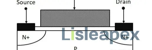
When current flows from the drain to the source, it mainly flows laterally within the silicon wafer, primarily through the top surface layer. As a result, the full size of the chip is not utilized. Furthermore, the breakdown voltage of this structure is determined by the width and doping of the P-layer beneath the gate. This region also serves as the conducting channel. To reduce the conduction resistance of the channel, the width of the P-layer beneath the gate cannot be too large, and the doping concentration cannot be too low.
Therefore, the breakdown voltage of this structure is generally low and cannot withstand high reverse voltages. Additionally, even if the cross-sectional area of the channel increases, the overall cross-sectional area of the chip remains small. Consequently, the current flows through a very small cross-sectional area of the chip, resulting in a high conduction resistance that limits the flow of large currents.
This structure's voltage and current ratings are limited, making it unsuitable for power circuits. However, this structure has low capacitance and short channel length, which makes it suitable for low-voltage applications such as microprocessors, memory chips, operational amplifiers, digital circuits, and radio frequency circuits.
In semiconductor manufacturing processes, chip or semiconductor feature sizes are often referred to, such as 3um, 2um, 1.5um, 1um, 0.8um, 0.5um, 0.35um, 0.25um, 0.18um, 0.13um, 90nm, 65nm, 45nm, 32nm, 22nm, 14nm, and 10nm. The process size typically refers to the width of the gate, the trench, or the linewidth. It does not represent the size of each individual cell.
The trench width corresponds to the distance between the drain and source. As the trench width decreases, the conduction time for carriers to traverse the channel reduces, allowing for higher operating switching frequencies. A smaller trench width allows for lower gate voltages to open the channel, resulting in easier conduction and reduced switching losses. Additionally, the channel conduction resistance decreases, leading to lower conduction losses.
However, as the spacing between the drain and source decreases, the contact area beneath the gate diminishes, weakening the gate's control over the channel. This leads to increased leakage current between the drain and source when the gate voltage is zero, resulting in device performance degradation and increased static power consumption. By utilizing double-gate structures and fin-shaped structures (FinFET), the issue of short-channel effects can be mitigated. This advancement promotes the continuous reduction of process sizes and enhances process capabilities in the next generation of chips.
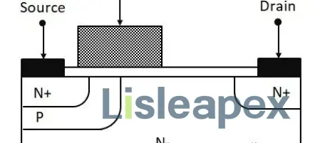
In single-chip power ICs, the integrated power MOSFETs can only use lateral conduction structures since all the pins are on the chip's surface. To address the low breakdown voltage issue between the drain and source, improvements must be made to the aforementioned structure. By introducing a lightly doped N-region, known as the drift layer or epitaxial layer, between the highly doped drain N+ region and the P-body channel. the flow of current can be directed from the N+ region to the N- region without affecting the conduction path.
Although the N- region is lightly doped, its resistivity is lower than that of the channel. By adjusting the doping concentration and width of the N- region, higher reverse voltages can be achieved while controlling the conduction resistance within the desired range. This structure allows for the conduction of large currents and is suitable for power circuits.
The N- layer added between the N+ drain and the P- body region is referred to as the "drift layer" or "epi layer." When a voltage is applied between the drain and source, the highly doped P-region forms a depletion layer primarily extending into the drift layer. The breakdown voltage between the drain and source relies heavily on the width and doping concentration of the drift layer.
By using the N- drift layer as the substrate, the structure shown in Figure 3 can be formed through two diffusion processes: the first diffusion process forms the P-well, also known as the P-body region, and the second diffusion process within the P-body region creates the N+ source. Therefore, this structure is called LDMOS (Lateral Double-Diffused MOSFET).
Although the majority carrier in the P-region is holes, local diffusion doping occurs in specific regions of the P-region. As long as the concentration of the 5-valence element used for doping is higher than the original concentration of the 3-valence element in the P-region, the electron concentration in the specific region will exceed the hole concentration, resulting in a transformation to an N-type semiconductor.
Therefore, the key factor in determining whether it is an N-type or P-type semiconductor lies not in the doping of multivalent elements but in the electron and hole concentrations. If the electron concentration is higher than the hole concentration in a specific region, the majority carriers are electrons, and the minority carriers are holes, indicating an N-type semiconductor. Conversely, it is a P-type semiconductor.
Structure of Vertical Conductive Double-Diffused Metal-Oxide-Semiconductor Field-Effect Transistor (MOSFET)
The chip has a very thin thickness, while the chip's area, relatively speaking, is large in size. As shown in Figure 3, the current still flows in the upper surface of the chip, laterally moving from the drain to the source. The cross-sectional area through which the current flows is small, resulting in high conduction resistance and underutilization of the chip's size.
Additionally, in order to increase the breakdown voltage between the drain and source, the width of the N-layer drift region must be increased, further increasing the conduction resistance and limiting the current-carrying capacity of the chip. Therefore, if designing high-voltage and high-current LDMOS, the chip size would be extremely large, leading to high costs. As a result, LDMOS is only used in low-voltage and low-current single-chip power ICs.
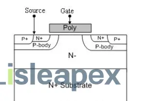
If we relocate the N+ drain region of the MOSFET structure in Figure 3 to the bottom of the substrate and extract the drain through the lower surface of the substrate, when the MOSFET is turned on, the current can flow vertically from the bottom drain to the top source through the inside of the chip. Moreover, the current flows through the entire horizontal cross-sectional area of the chip. Due to the larger horizontal cross-sectional area of the chip, the conduction resistance is reduced, thus enhancing the MOSFET's current-carrying capability.
In this structure, the lower the doping concentration and the greater the thickness of the N- epitaxial layer, the higher the breakdown voltage between the drain and source, and the larger the conduction resistance. Conversely, the higher the doping concentration and the smaller the thickness, the lower the breakdown voltage and the smaller the conduction resistance. By adjusting the doping concentration and thickness of the N- epitaxial layer, the desired breakdown voltage can be achieved while meeting the design requirements for conduction resistance.
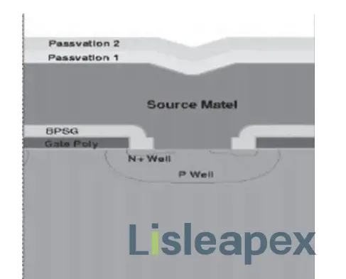
For this N-channel power MOSFET structure, an N+ heavily doped substrate is used, which has low resistance in the heavily doped region. A low-doped, high-purity, and highly consistent N- epitaxial layer is then formed on top of the N+ substrate. Within the N- epitaxial layer, two successive P-body regions and N+ source regions within these P-body regions are created through two diffusion processes. A thin, high-quality gate oxide is formed on the chip's surface, and polycrystalline silicon gate material is deposited on top of the oxide.
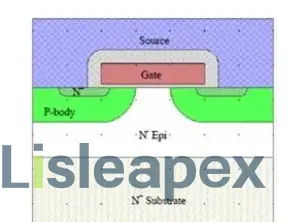
The channel is formed in the P-body region beneath the gate oxide, and metal material is deposited in the source and drain regions, completing the production of this structure. The current in this structure flows vertically from bottom to top and is achieved through two diffusion processes, hence the name Vertical Conductive Double-Diffused MOSFET (VDMOSFET). This structure does not require trench formation during the fabrication process; instead, it employs planar technology, also known as planar power MOSFET structure.
Its working principle is as follows: a forward voltage is applied between the gate and source, attracting minority carriers (electrons) in the P-region below the gate to the upper surface of the P-region beneath the gate due to the electric field. With an increasing forward bias voltage between the gate and source, more electrons are attracted to the thin-layer region on this surface.
This local electron density becomes larger than that of holes, resulting in "inversion" and forming an inversion layer. The semiconductor material changes from P-type to N-type, creating an N-type "channel" within the P-body region beneath the gate oxide. The current can flow directly from the N+ drain region, through the N- epitaxial layer and N-type channel beneath the gate oxide, to the N+ source region.
In reality, the structure diagram above only represents a single unit, also known as a "cell," within the internal structure of the power MOSFET. The internal structure of the power MOSFET consists of numerous such cells connected in parallel. The larger the chip area, the more units can be fabricated, resulting in lower device conduction resistance and higher current-carrying capacity.
Similarly, on a chip with a fixed area, the higher the unit density, i.e., the greater the number of cells that can be fabricated, the lower the conduction resistance of the device. The smaller the conduction resistance, the greater the current-carrying capacity and the higher the rated current.
In this structure, the area beneath the gate, where a large current does not flow through the main power circuit, cannot be fully utilized, which affects the maximum unit density that can be fabricated.
A larger gate area leads to larger parasitic capacitance (Crss), resulting in poor switching performance and higher switching losses. Additionally, inherent JFET (junction field-effect transistor) effects within the structure contribute to increased conduction resistance. However, this type of power MOSFET has a simple fabrication process and good unit consistency, resulting in favorable transconductance characteristics and high avalanche energy capability. It is mainly applied in high-voltage power MOSFETs and medium-voltage power MOSFETs with lower switching frequencies.
The region beneath the gate oxide layer is the N- epitaxial region, with two P-body regions on its sides. This inherent structure forms a JFET, as shown in Figure 8, resulting in JFET effects. The N-region and the P-regions on both sides form PN junctions, creating depletion layers and space charge regions. Even when the power MOSFET is conducting, this depletion layer still exists.
Therefore, the current mainly flows through the non-depleted region between the two P-regions, effectively reducing the cross-sectional area available for current conduction. This can be considered as an increase in conduction resistance due to JFET effects, referred to as JFET resistance. The wider the depletion layer, the smaller the channel area for current, and the more pronounced the JFET effects, resulting in larger JFET resistance.
The width of the depletion layer depends on the absolute value of the voltage between the gate (P-region) and the source (top region of the N- epitaxial layer). When this voltage is 0, the depletion layer is very narrow, resulting in very low JFET resistance. As this voltage increases, the depletion layer widens, and JFET resistance increases. Of course, JFET resistance is also influenced by the drain-source voltage of the power MOSFET.
訂閱時事通訊,了解 亮辰科技 的最新動態
