恭喜您提交成功
 提交失敗
提交失敗
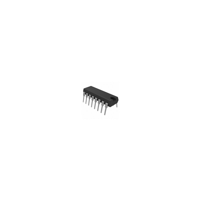
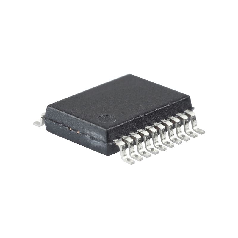
TDA1549T
D/A Converter, 18-Bit, 2 Func, CMOS, PDSO16
品質保證
品質保證
從我們的供應鍊網路採購的所有零件都經過嚴格的進貨檢驗流程。 這種細緻的檢查可確保客戶收到的零件是正品並符合要求的標準。 此外,我們還保存這些檢查的詳細記錄,以確保整個供應鏈的透明度和可追溯性。


認證
我們已成功獲得各項認證標準,並建立了自己的專業檢測實驗室。 這確保了我們向客戶提供的每件產品都符合最高的品質標準。 我們遵守嚴格的測試協議,以保持我們產品的一致性和準確性。 為了確保我們的產品是原裝正品,我們還與信譽良好的第三方檢測機構合作進行嚴格的品質測試。 我們對品質的承諾延伸到滿足行業、法律、監管和 ISO 9001:2015 的要求。
運輸與付款
運輸與付款
關於運送
我們通常會在幾個工作日內通過可靠的運輸公司(例如 FedEx、SF、UPS 或 DHL)運送訂單。 我們還支持其他運輸方式。 如果您想詢問具體的運輸細節或費用,請隨時與我們聯繫。


關於付款
我們接受多種支付方式,包括VISA、MasterCard、銀聯、西聯、PayPal等渠道。
如果您有特定的付款方式或想詢問費率和其他詳細信息,請隨時與我們聯繫。

電匯

Paypal

信用卡

西聯匯款

速匯金
服務與包裝
服務與包裝
About After Sales Service
All Parts Extended Quality Guarantee
自發貨之日起 90 天內發起申請。
與我們的工作人員確認退貨或換貨。
保持貨物收到時的原始狀態。
最後請注意,退貨或換貨的資格取決於對退貨商品實際狀況的評估。 在完成退貨或換貨流程之前,我們將評估收到的貨物。 如果您對退貨或換貨有任何疑問或需要進一步幫助,請隨時通過以下方式聯絡我們: [email protected]
關於包裝
在包裝方面,我們的產品均精心包裝在防靜電袋中,以提供ESD防靜電保護。 外包裝堅固耐用且閉合牢固。 我們支持各種包裝方法,例如捲帶式、切帶式、管式或託盤式。

例子

捲帶式

剪膠帶

管或託盤
TDA1549T 數據表

目前的價格方案正在編制中。請聯絡我們的客戶服務團隊獲取最新的價格資訊。感謝您的理解和支援!
詳細說明
GENERAL DESCRIPTIONThe TDA1549T (BCC-DAC1) is the first of a new generation of digital-to-analog converters featuring a unique combination of bitstream and continuous calibration concepts.FEATURES• Easy application• Finite-duration impulse-response (FIR) filtering and noise shaping incorporated• 2nd-order noise shaper• Wide dynamic range (true 18-bit resolution)• Low total harmonic distortion• No zero-crossing distortion• Superior signal-to-noise ratio• Bitstream continuous calibration conversion concept• Inherently monotonic• Voltage output (1.5 V RMS) at line drive level• Single supply rail (3.8 to 5.5 V)• Optimum output voltage level over the entire supply range• Small outline packaging (SO16)• Wide operating temperature range (−30 to +85 °C)• Standard Japanese input format• No analog post-filtering required• Low power consumption• Integrated operational amplifiers.

主要特徵
- Easy application
- Finite-duration impulse-response (FIR) filtering and noise shaping incorporated
- 2nd-order noise shaper
- Wide dynamic range (true 18-bit resolution)
- Low total harmonic distortion
- No zero-crossing distortion
- Superior signal-to-noise ratio
- Bitstream continuous calibration conversion concept
- Inherently monotonic
- Voltage output (1.5 V RMS) at line drive level
- Single supply rail (3.8 to 5.5 V)
- Optimum output voltage level over the entire supply range
- Small outline packaging (SO16)
- Wide operating temperature range (−30 to +85 °C)
- Standard Japanese input format
- No analog post-filtering required
- Low power consumption
- Integrated operational amplifiers.
規格
以下是所選零件的基本參數,涉及零件的特性及其所屬類別。
| Rohs Code | No | Part Life Cycle Code | Transferred |
| Reach Compliance Code | HTS Code ! | 8542.39.00.01 | |
| Converter Type | D/A CONVERTER | Input Bit Code | 2'S COMPLEMENT |
| JESD-30 Code | R-PDSO-G16 | JESD-609 Code | e0 |
| Number of Bits | 18 | Number of Functions | 2 |
| Number of Terminals | 16 | Operating Temperature-Max | 85 °C |
| Operating Temperature-Min | -30 °C | Package Body Material | PLASTIC/EPOXY |
| Package Code | SOP | Package Equivalence Code | SOP16,.4 |
| Package Shape | RECTANGULAR | Package Style | SMALL OUTLINE |
| Power Supplies ! | 5 V | Qualification Status ! | Not Qualified |
| Supply Voltage-Nom | 5 V | Surface Mount ! | YES |
| Technology | CMOS | Temperature Grade ! | OTHER |
| Terminal Finish | Tin/Lead (Sn/Pb) | Terminal Form ! | GULL WING |
| Terminal Pitch ! | 1.27 mm | Terminal Position | DUAL |
數據表 PDF
數據表記錄了器件的特性、絕對最大額定值、應用等,這對於作為器件特定應用的整體指南大有裨益。
常見問題解答
What is TDA1549T?
The TDA1549T is a stereo continuous calibration 16-bit digital-to-analog converter (DAC) designed by NXP Semiconductors. It is commonly used in audio applications such as CD players, digital audio systems, and multimedia devices to convert digital audio signals into high-quality analog audio output.
How Does TDA1549T Work?
The TDA1549T operates by converting digital audio signals into analog voltage outputs with high precision and linearity. It utilizes a 16-bit DAC architecture to ensure accurate signal conversion and reproduction. The DAC is designed for stereo applications, providing two channels of analog output for left and right audio channels.
How Many Pins does TDA1549T have and What are the Functions of the Pinout Configuration?
The TDA1549T is housed in a 16-pin DIL (Dual In-Line) package. The pinout configuration includes:
- VDD: Power supply pin.
- VSS: Ground pin.
- OSCL, OSCR: Clock input pins for the left and right channels, respectively.
- DATA: Serial data input pin for digital audio data.
- LRC: Left/right clock input for channel selection.
- LOUT: Analog output pin for the left channel.
- ROUT: Analog output pin for the right channel.
- Vref: Reference voltage pin for internal operations.
What are the Pros and Cons of TDA1549T?
Pros:
- High Resolution: Offers 16-bit resolution for accurate audio signal reproduction.
- Stereo Output: Provides dual-channel analog output for stereo audio applications.
- Continuous Calibration: Includes continuous calibration features for optimal performance over time.
- Low Distortion: Achieves low distortion and noise levels for high-quality audio output.
- Simple Interface: Interfaces easily with digital audio sources through a serial input.
Cons:
- External Components: May require external components for filtering and buffering to optimize audio performance.
- Limited Features: Compared to newer DACs, the TDA1549T may have fewer advanced features and specifications.
- Availability: As an older component, availability and support may be limited compared to newer DACs.
Are There Any Equivalents/Alternatives to TDA1549T for Recommendation?
- Alternatives to the TDA1549T include the PCM1794 from Texas Instruments and the CS43122 from Cirrus Logic, which offer similar audio performance and features.
- The Burr-Brown PCM1798 is another alternative with comparable audio quality and resolution.