恭喜您提交成功
 提交失敗
提交失敗
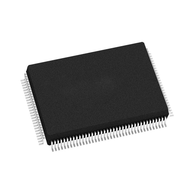
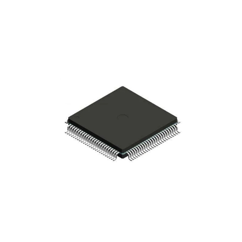
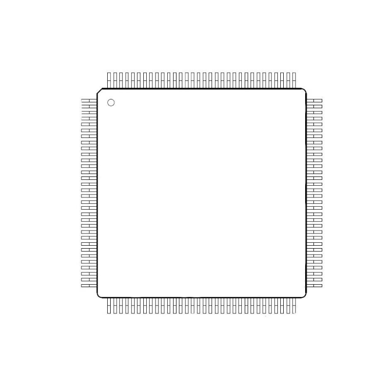
RTL8196E-CG
Realtek LQFP-128
品質保證
品質保證
從我們的供應鍊網路採購的所有零件都經過嚴格的進貨檢驗流程。 這種細緻的檢查可確保客戶收到的零件是正品並符合要求的標準。 此外,我們還保存這些檢查的詳細記錄,以確保整個供應鏈的透明度和可追溯性。


認證
我們已成功獲得各項認證標準,並建立了自己的專業檢測實驗室。 這確保了我們向客戶提供的每件產品都符合最高的品質標準。 我們遵守嚴格的測試協議,以保持我們產品的一致性和準確性。 為了確保我們的產品是原裝正品,我們還與信譽良好的第三方檢測機構合作進行嚴格的品質測試。 我們對品質的承諾延伸到滿足行業、法律、監管和 ISO 9001:2015 的要求。
運輸與付款
運輸與付款
關於運送
我們通常會在幾個工作日內通過可靠的運輸公司(例如 FedEx、SF、UPS 或 DHL)運送訂單。 我們還支持其他運輸方式。 如果您想詢問具體的運輸細節或費用,請隨時與我們聯繫。


關於付款
我們接受多種支付方式,包括VISA、MasterCard、銀聯、西聯、PayPal等渠道。
如果您有特定的付款方式或想詢問費率和其他詳細信息,請隨時與我們聯繫。

電匯

Paypal

信用卡

西聯匯款

速匯金
服務與包裝
服務與包裝
About After Sales Service
All Parts Extended Quality Guarantee
自發貨之日起 90 天內發起申請。
與我們的工作人員確認退貨或換貨。
保持貨物收到時的原始狀態。
最後請注意,退貨或換貨的資格取決於對退貨商品實際狀況的評估。 在完成退貨或換貨流程之前,我們將評估收到的貨物。 如果您對退貨或換貨有任何疑問或需要進一步幫助,請隨時通過以下方式聯絡我們: [email protected]
關於包裝
在包裝方面,我們的產品均精心包裝在防靜電袋中,以提供ESD防靜電保護。 外包裝堅固耐用且閉合牢固。 我們支持各種包裝方法,例如捲帶式、切帶式、管式或託盤式。

例子

捲帶式

剪膠帶

管或託盤
RTL8196E-CG 數據表
價格 (USD)
| 數量 | 單價 | 總價 |
|---|---|---|
| 1 | $2.145 | $2.14 |
| 10 | $1.868 | $18.68 |
| 30 | $1.695 | $50.85 |
| 90 | $1.451 | $130.59 |
| 540 | $1.370 | $739.80 |
| 990 | $1.336 | $1,322.64 |
這些價格會受到市場波動的影響,需要提交報價才能取得最新價格。
詳細說明
General DescriptionThe RTL8196E-CG is an integrated System-on-a-Chip (SoC) Application Specific Integrated Circuit (ASIC) L2 5-Port Ethernet switch. An RLX4181 CPU is embedded and the clock rate can be up to 400MHz. To improve computational performance, a 16Kbyte I-Cache, 8Kbyte D-Cache, 16Kbyte I-MEM, and 8Kbyte D-MEM are provided. A standard 5-signal P1149.1 compliant EJTAG test interface is supported for CPU testing and software development.Features■ SOC ◆ Embedded RISC CPU, RLX4181 with 16Kbyte I-Cache, 8Kbyte D-Cache, 16Kbyte I-MEM, 8Kbyte D-MEM ◆ Supports MIPS-1 ISA, MIPS16 ISA ◆ Clock Rate: 400MHz ◆ Provides a standard P1149.1 EJTAG test port ◆ Supports RLX4181 CPU suspend mode■ L2 Capabilities ◆ Five Ethernet MAC switch with five IEEE 802.3 10/100M physical layer transceivers ◆ Non-blocking wire-speed reception and transmission and non-head-of-line blocking/forwarding ◆ Internal 256Kbit SRAM for packet buffering ◆ Internal 1024 entry 4-way hash L2 look up table ◆ Supports source and destination MAC address filtering■ CPU Interface (NIC) ◆ Supports BSD mbuf-like packet structure with adjustable cluster size (128-byte to 2Kbyte) to provide optimum memory utilization ◆ The NIC DMA supports multiple descriptor-ring architecture for QoS applications■ Peripheral Interfaces ◆ Supports PCI Express Host with integrated PHY ◆ One PCI Express PHY embedded ◆ Supports one-port USB ■ USB 2.0 Host or Device ◆ One USB PHY embedded ◆ Supports two 16550 UARTs ◆ Supports up to 16 GPIO pins■ Memory Interfaces ◆ Serial Flash (SPI Type) ■ Supports one bank and dual I/O channels for SPI Flash application ■ Each Flash bank could be configured as 256K/512K/1M/2M/4M/8M/16M Bytes ■ Boot up from SPI flash is supported ◆ SDR DRAM ■ Supports one SDR DRAM bank; each can be configured as 2M/4M/8M/16M/32M/64Mbyte ■ 16-bit SDR DRAM data bus supported ◆ DDR1 DRAM ■ Supports one DDR1 DRAM bank that can be configured as 16M/32M/64M/128Mbytes ■ 16-bit DDR1 DRAM data bus supported. System totally supports up to 128Mbyte DDR1 DRAM memory space ◆ DDR2 DRAM ■ Supports one DDR2 DRAM bank that can be configured as 32M/64M/128Mbyte ■ 16-bit DDR2 DRAM data bus supported. System totally supports up to 128Mbyte DDR2 DRAM memory space■ Supports Green Ethernet ◆ Cable length power saving ◆ Link down power saving■ Supports IEEE 802.3az Energy Efficient Ethernet ability for 100Base-TX in full duplex operation and 10Base-T in full/half duplex mode■ Other Added-Value Features ◆ Supports Link Down Power Saving in Ethernet PHYceivers ◆ Supports two hardware timers and one watchdog timer ◆ Per-port configurable auto-crossover function ◆ Built-in internal ROM booting ◆ Single 25MHz crystal or 40MHz clock input■ Built-in SWR/LDO ◆ LDO for DDR1/DDR2 ■ DDR1 DRAM: 3.3V to 2.5V ■ DDR2 DRAM: 3.3V to 1.8V ◆ SWR or LDO for Core Power ■ SWR or LDO 3.3V to 1.0V■ LQFP128 packageSystem Applications■ IEEE 802.11b/g/n AP/Router■ IEEE 802.11a/b/g/n Dualband Concurrent Router■ Wired Router

主要特徵
- SOC
- Embedded RISC CPU, RLX4181 with
- 16Kbyte I-Cache, 8Kbyte D-Cache,
- 16Kbyte I-MEM, 8Kbyte D-MEM
- Supports MIPS-1 ISA, MIPS16 ISA
- Clock Rate: 400MHz
- Provides a standard P1149.1 EJTAG test
- port
- Supports RLX4181 CPU suspend mode
- L2 Capabilities
- Five Ethernet MAC switch with five
- IEEE 802.3 10/100M physical layer
- transceivers
- Non-blocking wire-speed reception and
- transmission and non-head-of-line
- blocking/forwarding
- Internal 256Kbit SRAM for packet
- buffering
- Internal 1024 entry 4-way hash L2 look
- up table
- Supports source and destination MAC
- address filtering
- CPU Interface (NIC)
- Supports BSD mbuf-like packet structure
- with adjustable cluster size (128-byte to
- 2Kbyte) to provide optimum memory
- utilization
- The NIC DMA supports multiple
- descriptor-ring architecture for QoS
- applications
- Peripheral Interfaces
- Supports PCI Express Host with
- integrated PHY
- One PCI Express PHY embedded
- Supports one-port USB
- USB 2.0 Host or Device
- One USB PHY embedded
- Supports two 16550 UARTs
- Supports up to 16 GPIO pins
- Memory Interfaces
- Serial Flash (SPI Type)
- Supports one bank and dual I/O
- channels for SPI Flash application
- Each Flash bank could be configured
- as 256K/512K/1M/2M/4M/8M/16M
- Bytes
- Boot up from SPI flash is supported
- SDR DRAM
- Supports one SDR DRAM bank; each
- can be configured as
- 2M/4M/8M/16M/32M/64Mbyte
- 16-bit SDR DRAM data bus
- supported
- DDR1 DRAM
- Supports one DDR1 DRAM bank
- that can be configured as
- 16M/32M/64M/128Mbytes
- 16-bit DDR1 DRAM data bus
- supported. System totally supports up
- to 128Mbyte DDR1 DRAM memory
- space
- DDR2 DRAM
- Supports one DDR2 DRAM bank
- that can be configured as
- 32M/64M/128Mbyte
- 16-bit DDR2 DRAM data bus
- supported. System totally supports up
- to 128Mbyte DDR2 DRAM memory
- space
- Supports Green Ethernet
- Cable length power saving
- Link down power saving
- Supports IEEE 802.3az Energy Efficient
- Ethernet ability for 100Base-TX in full
- duplex operation and 10Base-T in full/half
- duplex mode
- Other Added-Value Features
- Supports Link Down Power Saving in
- Ethernet PHYceivers
- Supports two hardware timers and one
- watchdog timer
- Per-port configurable auto-crossover
- function
- Built-in internal ROM booting
- Single 25MHz crystal or 40MHz clock
- input
- Built-in SWR/LDO
- LDO for DDR1/DDR2
- DDR1 DRAM: 3.3V to 2.5V
- DDR2 DRAM: 3.3V to 1.8V
- SWR or LDO for Core Power
- SWR or LDO 3.3V to 1.0V
- LQFP128 package

規格
以下是所選零件的基本參數,涉及零件的特性及其所屬類別。
| Manufacturer | REALTEK | Product Category ! | IC Chips |
數據表 PDF
數據表記錄了器件的特性、絕對最大額定值、應用等,這對於作為器件特定應用的整體指南大有裨益。