恭喜您提交成功
 提交失敗
提交失敗
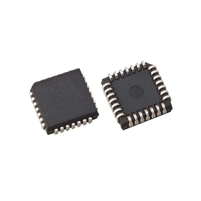
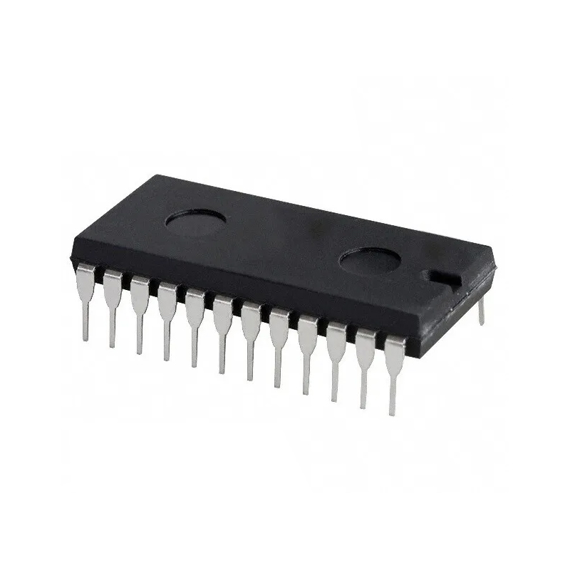
P89LPC932BA
Microcontroller, 8-Bit, FLASH, 8051 CPU, 12MHz, CMOS, PQCC28,P89LPC932BA
Microcontroller, 8-Bit, FLASH, 8051 CPU, 12MHz, CMOS, PQCC28,
品質保證
品質保證
從我們的供應鍊網路採購的所有零件都經過嚴格的進貨檢驗流程。 這種細緻的檢查可確保客戶收到的零件是正品並符合要求的標準。 此外,我們還保存這些檢查的詳細記錄,以確保整個供應鏈的透明度和可追溯性。


認證
我們已成功獲得各項認證標準,並建立了自己的專業檢測實驗室。 這確保了我們向客戶提供的每件產品都符合最高的品質標準。 我們遵守嚴格的測試協議,以保持我們產品的一致性和準確性。 為了確保我們的產品是原裝正品,我們還與信譽良好的第三方檢測機構合作進行嚴格的品質測試。 我們對品質的承諾延伸到滿足行業、法律、監管和 ISO 9001:2015 的要求。
運輸與付款
運輸與付款
關於運送
我們通常會在幾個工作日內通過可靠的運輸公司(例如 FedEx、SF、UPS 或 DHL)運送訂單。 我們還支持其他運輸方式。 如果您想詢問具體的運輸細節或費用,請隨時與我們聯繫。


關於付款
我們接受多種支付方式,包括VISA、MasterCard、銀聯、西聯、PayPal等渠道。
如果您有特定的付款方式或想詢問費率和其他詳細信息,請隨時與我們聯繫。

電匯

Paypal

信用卡

西聯匯款

速匯金
服務與包裝
服務與包裝
About After Sales Service
All Parts Extended Quality Guarantee
自發貨之日起 90 天內發起申請。
與我們的工作人員確認退貨或換貨。
保持貨物收到時的原始狀態。
最後請注意,退貨或換貨的資格取決於對退貨商品實際狀況的評估。 在完成退貨或換貨流程之前,我們將評估收到的貨物。 如果您對退貨或換貨有任何疑問或需要進一步幫助,請隨時通過以下方式聯絡我們: [email protected]
關於包裝
在包裝方面,我們的產品均精心包裝在防靜電袋中,以提供ESD防靜電保護。 外包裝堅固耐用且閉合牢固。 我們支持各種包裝方法,例如捲帶式、切帶式、管式或託盤式。

例子

捲帶式

剪膠帶

管或託盤
P89LPC932BA 數據表

目前的價格方案正在編制中。請聯絡我們的客戶服務團隊獲取最新的價格資訊。感謝您的理解和支援!
詳細說明
General descriptionThe P89LPC932 is a single-chip microcontroller, available in low cost packages, based on a high performance processor architecture that executes instructions in two to four clocks, six times the rate of standard 80C51 devices. Many system-level functions have been incorporated into the P89LPC932 in order to reduce component count, board space, and system cost.Features■ A high performance 80C51 CPU provides instruction cycle times of 167-333 ns for all instructions except multiply and divide when executing at 12 MHz. This is 6 times the performance of the standard 80C51 running at the same clock frequency. A lower clock frequency for the same performance results in power savings and reduced EMI.■ 2.4 V to 3.6 V VDD operating range. I/O pins are 5 V tolerant (may be pulled up or driven to 5.5 V).■ 8 kB Flash code memory with 1 kB erasable sectors, 64-byte erasable page size.■ 256-byte RAM data memory. 512-byte auxiliary on-chip RAM.■ 512-byte customer Data EEPROM on chip allows serialization of devices, storage of set-up parameters, etc.■ Two 16-bit counter/timers. Each timer may be configured to toggle a port output upon timer overflow or to become a PWM output.■ Real-Time clock that can also be used as a system timer.■ Capture/Compare Unit (CCU) provides PWM, input capture, and output compare functions.■ Two analog comparators with selectable inputs and reference source.■ Enhanced UART with fractional baud rate generator, break detect, framing error detection, automatic address detection and versatile interrupt capabilities.■ 400 kHz byte-wide I2C-bus communication port.■ SPI communication port.■ Eight keypad interrupt inputs, plus two additional external interrupt inputs.■ Four interrupt priority levels.■ Watchdog timer with separate on-chip oscillator, requiring no external components. The watchdog prescaler is selectable from 8 values.■ Active-LOW reset. On-chip power-on reset allows operation without external reset components. A reset counter and reset glitch suppression circuitry prevent spurious and incomplete resets. A software reset function is also available.■ Low voltage reset (Brownout detect) allows a graceful system shutdown when power fails. May optionally be configured as an interrupt.■ Oscillator Fail Detect. The Watchdog timer has a separate fully on-chip oscillator allowing it to perform an oscillator fail detect function.■ Configurable on-chip oscillator with frequency range and RC oscillator options (selected by user programmed Flash configuration bits). The RC oscillator option allows operation without external oscillator components. Oscillator options support frequencies from 20 kHz to the maximum operating frequency of 12 MHz. The RC oscillator option is selectable and fine tunable.■ Programmable port output configuration options: ◆ quasi-bidirectional, ◆ open drain, ◆ push-pull, ◆ input-only.■ Port ‘input pattern match’ detect. Port 0 may generate an interrupt when the value of the pins match or do not match a programmable pattern.■ Second data pointer.■ Schmitt trigger port inputs.■ LED drive capability (20 mA) on all port pins. A maximum limit is specified for the entire chip.■ Controlled slew rate port outputs to reduce EMI. Outputs have approximately 10 ns minimum ramp times.■ 23 I/O pins minimum (28-pin package). Up to 26 I/O pins while using on-chip oscillator and reset options.■ Only power and ground connections are required to operate the P89LPC932 when on-chip oscillator and reset options are selected.■ Serial Flash programming allows simple in-circuit production coding. Flash security bits prevent reading of sensitive application programs.■ In-Application Programming of the Flash code memory. This allows changing the code in a running application.■ Idle and two different Power-down reduced power modes. Improved wake-up from Power-down mode (a low interrupt input starts execution). Typical Power-down current is 1 µA (total Power-down with voltage comparators disabled).■ 28-pin PLCC, TSSOP, and HVQFN packages.■ Emulation support.

主要特徵
- A high performance 80C51 CPU provides instruction cycle times of 167-333 ns for all instructions except multiply and divide when executing at 12 MHz. This is 6 times the performance of the standard 80C51 running at the same clock frequency. A lower clock frequency for the same performance results in power savings and reduced EMI.
- 2.4 V to 3.6 V VDD operating range. I/O pins are 5 V tolerant (may be pulled up or driven to 5.5 V).
- 8 kB Flash code memory with 1 kB erasable sectors, 64-byte erasable page size.
- 256-byte RAM data memory. 512-byte auxiliary on-chip RAM.
- 512-byte customer Data EEPROM on chip allows serialization of devices, storage of set-up parameters, etc.
- Two 16-bit counter/timers. Each timer may be configured to toggle a port output upon timer overflow or to become a PWM output.
- Real-Time clock that can also be used as a system timer.
- Capture/Compare Unit (CCU) provides PWM, input capture, and output compare functions.
- Two analog comparators with selectable inputs and reference source.
- Enhanced UART with fractional baud rate generator, break detect, framing error detection, automatic address detection and versatile interrupt capabilities.
- 400 kHz byte-wide I2C-bus communication port.
- SPI communication port.
- Eight keypad interrupt inputs, plus two additional external interrupt inputs.
- Four interrupt priority levels.
- Watchdog timer with separate on-chip oscillator, requiring no external components. The watchdog prescaler is selectable from 8 values.
- Active-LOW reset. On-chip power-on reset allows operation without external reset components. A reset counter and reset glitch suppression circuitry prevent spurious and incomplete resets. A software reset function is also available.
- Low voltage reset (Brownout detect) allows a graceful system shutdown when power fails. May optionally be configured as an interrupt.
- Oscillator Fail Detect. The Watchdog timer has a separate fully on-chip oscillator allowing it to perform an oscillator fail detect function.
- Configurable on-chip oscillator with frequency range and RC oscillator options (selected by user programmed Flash configuration bits). The RC oscillator option allows operation without external oscillator components. Oscillator options support frequencies from 20 kHz to the maximum operating frequency of 12 MHz. The RC oscillator option is selectable and fine tunable.
- Programmable port output configuration options:
- quasi-bidirectional,
- open drain,
- push-pull,
- input-only.
- Port ‘input pattern match’ detect. Port 0 may generate an interrupt when the value of the pins match or do not match a programmable pattern.
- Second data pointer.
- Schmitt trigger port inputs.
- LED drive capability (20 mA) on all port pins. A maximum limit is specified for the entire chip.
- Controlled slew rate port outputs to reduce EMI. Outputs have approximately 10 ns minimum ramp times.
- 23 I/O pins minimum (28-pin package). Up to 26 I/O pins while using on-chip oscillator and reset options.
- Only power and ground connections are required to operate the P89LPC932 when on-chip oscillator and reset options are selected.
- Serial Flash programming allows simple in-circuit production coding. Flash security bits prevent reading of sensitive application programs.
- In-Application Programming of the Flash code memory. This allows changing the code in a running application.
- Idle and two different Power-down reduced power modes. Improved wake-up from Power-down mode (a low interrupt input starts execution). Typical Power-down current is 1 µA (total Power-down with voltage comparators disabled).
- 28-pin PLCC, TSSOP, and HVQFN packages.
- Emulation support.
規格
以下是所選零件的基本參數,涉及零件的特性及其所屬類別。
| Rohs Code | Yes | Part Life Cycle Code | Transferred |
| Reach Compliance Code | HTS Code ! | 8542.31.00.01 | |
| Bit Size | 8 | CPU Family | 8051 |
| JESD-30 Code | S-PQCC-J28 | Moisture Sensitivity Level | 3 |
| Number of Terminals | 28 | Operating Temperature-Max | 70 °C |
| Operating Temperature-Min | Package Body Material | PLASTIC/EPOXY | |
| Package Code | QCCJ | Package Equivalence Code | LDCC28,.5SQ |
| Package Shape | SQUARE | Package Style | CHIP CARRIER |
| Peak Reflow Temperature (Cel) | 245 | Power Supplies ! | 2.5/3.3 V |
| Qualification Status ! | Not Qualified | RAM (bytes) | 768 |
| ROM (words) | 8192 | ROM Programmability | FLASH |
| Speed | 12 MHz | Supply Current-Max | 18 mA |
| Surface Mount ! | YES | Technology | CMOS |
| Temperature Grade ! | COMMERCIAL | Terminal Form ! | J BEND |
| Terminal Pitch ! | 1.27 mm | Terminal Position | QUAD |
Specification Comparison
數據表 PDF
數據表記錄了器件的特性、絕對最大額定值、應用等,這對於作為器件特定應用的整體指南大有裨益。