恭喜您提交成功
 提交失敗
提交失敗

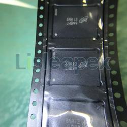
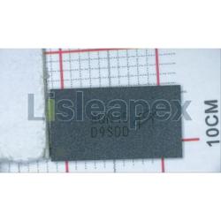
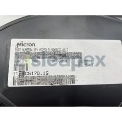
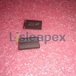
MT29F1G08ABAEAWP
IC FLASH 1GBIT PARALLEL 48TSOP I
品質保證
品質保證
從我們的供應鍊網路採購的所有零件都經過嚴格的進貨檢驗流程。 這種細緻的檢查可確保客戶收到的零件是正品並符合要求的標準。 此外,我們還保存這些檢查的詳細記錄,以確保整個供應鏈的透明度和可追溯性。


認證
我們已成功獲得各項認證標準,並建立了自己的專業檢測實驗室。 這確保了我們向客戶提供的每件產品都符合最高的品質標準。 我們遵守嚴格的測試協議,以保持我們產品的一致性和準確性。 為了確保我們的產品是原裝正品,我們還與信譽良好的第三方檢測機構合作進行嚴格的品質測試。 我們對品質的承諾延伸到滿足行業、法律、監管和 ISO 9001:2015 的要求。
運輸與付款
運輸與付款
關於運送
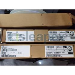
我們通常會在幾個工作日內通過可靠的運輸公司(例如 FedEx、SF、UPS 或 DHL)運送訂單。 我們還支持其他運輸方式。 如果您想詢問具體的運輸細節或費用,請隨時與我們聯繫。


關於付款
我們接受多種支付方式,包括VISA、MasterCard、銀聯、西聯、PayPal等渠道。
如果您有特定的付款方式或想詢問費率和其他詳細信息,請隨時與我們聯繫。

電匯

Paypal

信用卡

西聯匯款

速匯金
服務與包裝
服務與包裝
About After Sales Service
All Parts Extended Quality Guarantee
自發貨之日起 90 天內發起申請。
與我們的工作人員確認退貨或換貨。
保持貨物收到時的原始狀態。
最後請注意,退貨或換貨的資格取決於對退貨商品實際狀況的評估。 在完成退貨或換貨流程之前,我們將評估收到的貨物。 如果您對退貨或換貨有任何疑問或需要進一步幫助,請隨時通過以下方式聯絡我們: [email protected]
關於包裝
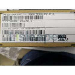
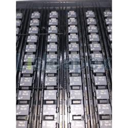
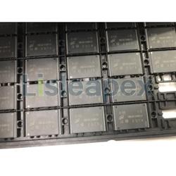
在包裝方面,我們的產品均精心包裝在防靜電袋中,以提供ESD防靜電保護。 外包裝堅固耐用且閉合牢固。 我們支持各種包裝方法,例如捲帶式、切帶式、管式或託盤式。

例子

捲帶式

剪膠帶

管或託盤
MT29F1G08ABAEAWP 數據表

目前的價格方案正在編制中。請聯絡我們的客戶服務團隊獲取最新的價格資訊。感謝您的理解和支援!
詳細說明
General DescriptionMicron NAND Flash devices include an asynchronous data interface for high-performance I/O operations. These devices use a highly multiplexed 8-bit bus (I/Ox) to transfer commands, address, and data. There are five control signals used to implement the asynchronous data interface: CE#, CLE, ALE, WE#, and RE#. Additional signals control hardware write protection and monitor device status (R/B#).This hardware interface creates a low pin-count device with a standard pinout that remains the same from one density to another, enabling future upgrades to higher densi ties with no board redesign.A target is the unit of memory accessed by a chip enable signal. A target contains one or more NAND Flash die. A NAND Flash die is the minimum unit that can independently execute commands and report status. A NAND Flash die, in the ONFI specification, is referred to as a logical unit (LUN). There is at least one NAND Flash die per chip enable signal. For further details, see Device and Array Organization.This device has an internal 4-bit ECC that can be enabled using the GET/SET features.See Internal ECC and Spare Area Mapping for ECC for more information.Features• Open NAND Flash Interface (ONFI) 1.0-compliant1• Single-level cell (SLC) technology• Organization – Page size x8: 2112 bytes (2048 + 64 bytes) – Page size x16: 1056 words (1024 + 32 words) – Block size: 64 pages (128K + 4K bytes) – Plane size: 2 planes x 2048 blocks per plane – Device size: 4Gb: 4096 blocks; 8Gb: 8192 blocks 16Gb: 16,384 blocks• Asynchronous I/O performance – tRC/tWC: 20ns (3.3V), 25ns (1.8V)• Array performance – Read page: 25µs 3 – Program page: 200µs (TYP: 1.8V, 3.3V)3 – Erase block: 700µs (TYP)• Command set: ONFI NAND Flash Protocol• Advanced command set – Program page cache mode4 – Read page cache mode 4 – One-time programmable (OTP) mode – Two-plane commands 4 – Interleaved die (LUN) operations – Read unique ID – Block lock (1.8V only) – Internal data move• Operation status byte provides software method for detecting – Operation completion – Pass/fail condition – Write-protect status• Ready/Busy# (R/B#) signal provides a hardware method of detecting operation completion• WP# signal: Write protect entire device• First block (block address 00h) is valid when ship ped from factory with ECC. For minimum required ECC, see Error Management.• Block 0 requires 1-bit ECC if PROGRAM/ERASE cycles are less than 1000• RESET (FFh) required as first command after power-on• Alternate method of device initialization (Nand_In it) after power up (contact factory)• Internal data move operations supported within the plane from which data is read• Quality and reliability – Data retention: 10 years – Endurance: 100,000 PROGRAM/ERASE cycles• Operating voltage range – VCC: 2.7–3.6V – VCC: 1.7–1.95V• Operating temperature: – Commercial: 0°C to +70°C – Industrial (IT): –40ºC to +85ºC• Package – 48-pin TSOP type 1, CPL2 – 63-ball VFBGA
主要特徵
- Open NAND Flash Interface (ONFI) 1.0-compliant1
- Single-level cell (SLC) technology
- Organization
- – Page size x8: 2112 bytes (2048 + 64 bytes)
- – Page size x16: 1056 words (1024 + 32 words)
- – Block size: 64 pages (128K + 4K bytes)
- – Plane size: 2 planes x 2048 blocks per plane
- – Device size: 4Gb: 4096 blocks; 8Gb: 8192 blocks 16Gb: 16,384 blocks
- Asynchronous I/O performance
- – tRC/tWC: 20ns (3.3V), 25ns (1.8V)
- Array performance
- – Read page: 25µs 3
- – Program page: 200µs (TYP: 1.8V, 3.3V)3
- – Erase block: 700µs (TYP)
- Command set: ONFI NAND Flash Protocol
- Advanced command set
- – Program page cache mode4
- – Read page cache mode 4
- – One-time programmable (OTP) mode
- – Two-plane commands 4
- – Interleaved die (LUN) operations
- – Read unique ID
- – Block lock (1.8V only)
- – Internal data move
- Operation status byte provides software method for detecting
- – Operation completion
- – Pass/fail condition
- – Write-protect status
- Ready/Busy# (R/B#) signal provides a hardware method of detecting operation completion
- WP# signal: Write protect entire device
- First block (block address 00h) is valid when ship ped from factory with ECC. For minimum required ECC, see Error Management.
- Block 0 requires 1-bit ECC if PROGRAM/ERASE cycles are less than 1000
- RESET (FFh) required as first command after power-on
- Alternate method of device initialization (Nand_In it) after power up (contact factory)
- Internal data move operations supported within the plane from which data is read
- Quality and reliability
- – Data retention: 10 years
- – Endurance: 100,000 PROGRAM/ERASE cycles
- Operating voltage range
- – VCC: 2.7–3.6V
- – VCC: 1.7–1.95V
- Operating temperature:
- – Commercial: 0°C to +70°C
- – Industrial (IT): –40ºC to +85ºC
- Package
- – 48-pin TSOP type 1, CPL2
- – 63-ball VFBGA

規格
以下是所選零件的基本參數,涉及零件的特性及其所屬類別。
| Category | Integrated Circuits (ICs)MemoryMemory | Mfr | Micron Technology Inc. |
| Series | - | Package | Tape & Reel (TR)Cut Tape (CT)® |
| Product Status | Active | Programmable | Verified |
| Memory Type ! | Non-Volatile | Memory Format | FLASH |
| Technology | FLASH - NAND | Memory Size ! | 1Gbit |
| Memory Organization | 128M x 8 | Memory Interface ! | Parallel |
| Write Cycle Time - Word, Page | - | Voltage - Supply | 2.7V ~ 3.6V |
| Operating Temperature ! | -40°C ~ 85°C (TA) | Mounting Type | Surface Mount |
| Package / Case | 48-TFSOP (0.724", 18.40mm Width) | Supplier Device Package | 48-TSOP I |
| Base Product Number | MT29F1G08 |
Specification Comparison
推薦零件
-
![MTFC4GACAAAM-4M IT]()
3,482 有存貨
貨物週期: 3~7 天
最小訂購量為 1
-
![MT41K128M16JT-125]()
4,405 有存貨
貨物週期: 3~7 天
最小訂購量為 1
-
![MT47H128M8SH-25E IT:M]()
MT47H128M8SH-25E IT:M
$1.892 IT:M MT47H128M8SH-25E DDR2 Memory Component
製造商: Micron Technology 包裝/箱: FBGA-60
4,353 有存貨
貨物週期: 3~7 天
最小訂購量為 1
-
![MT41K256M16LY-093:N]()
FBGA 96-Pin DRAM Chip for DDR3L SDRAM with 1.35V voltage
製造商: Alliance Memory 包裝/箱: FBGA-96
5,739 有存貨
貨物週期: 3~7 天
最小訂購量為 1
-
![MT25QL512ABB1EW9-0SIT]()
MT25QL512ABB1EW9-0SIT
$4.027 This product is a FLASH memory chip with a capacity of 512MX1, packaged in a PDSO8 form factor
製造商: Micron 包裝/箱: WDFN-8
3,709 有存貨
貨物週期: 3~7 天
最小訂購量為 1
-
![MTFC4GACAAAM-1M WT]()
4,248 有存貨
貨物週期: 3~7 天
最小訂購量為 1
-
![MT41K256M16LY-107:N]()
5,047 有存貨
貨物週期: 3~7 天
最小訂購量為 1
-
![MT25QL512ABB8ESF-0SIT]()
3,620 有存貨
貨物週期: 3~7 天
最小訂購量為 1
-
![MT25QL01GBBB8E12-0SIT]()
5,232 有存貨
貨物週期: 3~7 天
最小訂購量為 1
-
![MT28EW01GABA1HJS-0SIT]()
4,786 有存貨
貨物週期: 3~7 天
最小訂購量為 1
-
![MT28EW512ABA1HJS-0SIT]()
6,170 有存貨
貨物週期: 3~7 天
最小訂購量為 1
-
![MT41K1G16DGA-125:A]()
4,408 有存貨
貨物週期: 3~7 天
最小訂購量為 1
-
![MT29F4G08ABBDAH4]()
Store more, worry less with Micron Technology's advanced MT29F4G08ABBDAH4 NAND flash memory solution for your digital requirements
製造商: MICRON 包裝/箱: VFBGA-63
4,657 有存貨
貨物週期: 3~7 天
最小訂購量為 1
-
![MT29F4G08AACWC:C]()
6,217 有存貨
貨物週期: 3~7 天
最小訂購量為 1