恭喜您提交成功
 提交失敗
提交失敗

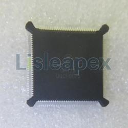
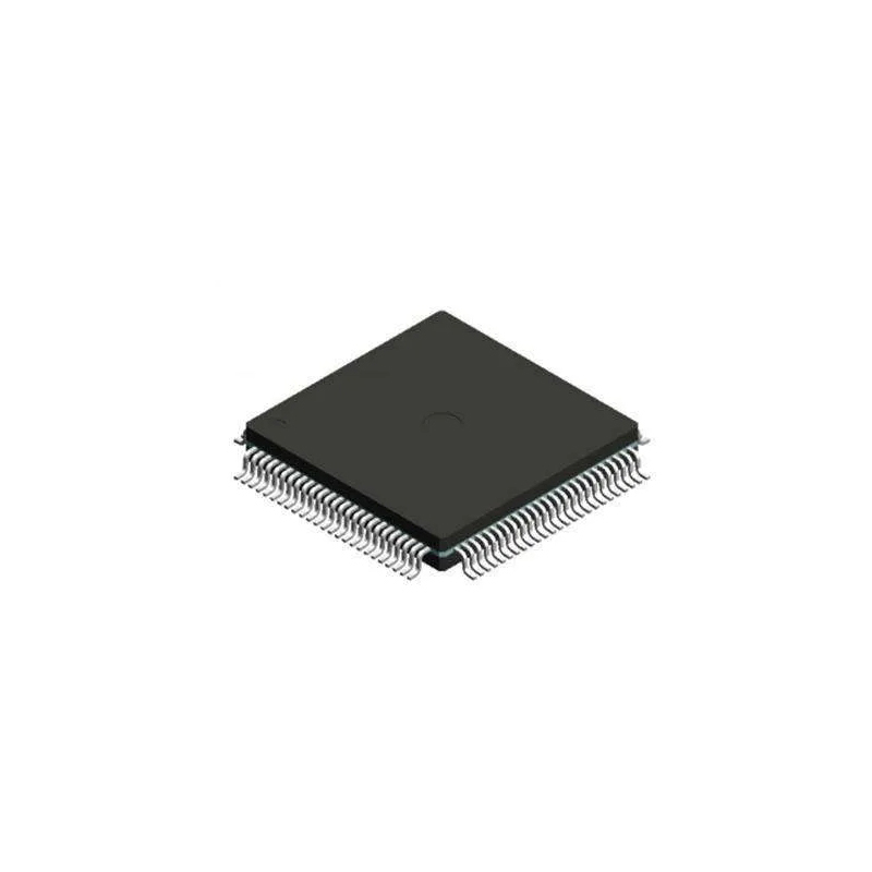
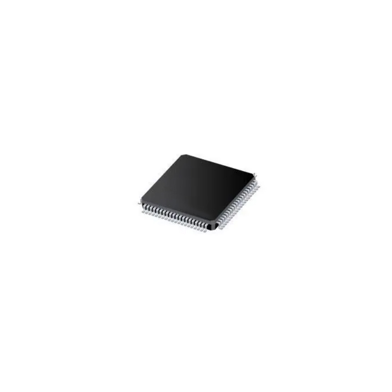
MC56F8035V
16-bit Digital Signal Controllers
品質保證
品質保證
從我們的供應鍊網路採購的所有零件都經過嚴格的進貨檢驗流程。 這種細緻的檢查可確保客戶收到的零件是正品並符合要求的標準。 此外,我們還保存這些檢查的詳細記錄,以確保整個供應鏈的透明度和可追溯性。


認證
我們已成功獲得各項認證標準,並建立了自己的專業檢測實驗室。 這確保了我們向客戶提供的每件產品都符合最高的品質標準。 我們遵守嚴格的測試協議,以保持我們產品的一致性和準確性。 為了確保我們的產品是原裝正品,我們還與信譽良好的第三方檢測機構合作進行嚴格的品質測試。 我們對品質的承諾延伸到滿足行業、法律、監管和 ISO 9001:2015 的要求。
運輸與付款
運輸與付款
關於運送
我們通常會在幾個工作日內通過可靠的運輸公司(例如 FedEx、SF、UPS 或 DHL)運送訂單。 我們還支持其他運輸方式。 如果您想詢問具體的運輸細節或費用,請隨時與我們聯繫。


關於付款
我們接受多種支付方式,包括VISA、MasterCard、銀聯、西聯、PayPal等渠道。
如果您有特定的付款方式或想詢問費率和其他詳細信息,請隨時與我們聯繫。

電匯

Paypal

信用卡

西聯匯款

速匯金
服務與包裝
服務與包裝
About After Sales Service
All Parts Extended Quality Guarantee
自發貨之日起 90 天內發起申請。
與我們的工作人員確認退貨或換貨。
保持貨物收到時的原始狀態。
最後請注意,退貨或換貨的資格取決於對退貨商品實際狀況的評估。 在完成退貨或換貨流程之前,我們將評估收到的貨物。 如果您對退貨或換貨有任何疑問或需要進一步幫助,請隨時通過以下方式聯絡我們: [email protected]
關於包裝
在包裝方面,我們的產品均精心包裝在防靜電袋中,以提供ESD防靜電保護。 外包裝堅固耐用且閉合牢固。 我們支持各種包裝方法,例如捲帶式、切帶式、管式或託盤式。

例子

捲帶式

剪膠帶

管或託盤
MC56F8035V 數據表

目前的價格方案正在編制中。請聯絡我們的客戶服務團隊獲取最新的價格資訊。感謝您的理解和支援!
詳細說明
56F8035/56F8025 Description The 56F8035/56F8025 is a member of the 56800E core-based family of Digital Signal Controllers (DSCs). It combines, on a single chip, the processing power of a DSP and the functionality of a microcontroller with a flexible set of peripherals to create an extremely cost-effective solution. Because of its low cost, configuration flexibility, and compact program code, the 56F8035/56F8025 is well-suited for many applications. The 56F8035/56F8025 includes many peripherals that are especially useful for industrial control, motion control, home appliances, general-purpose inverters, smart sensors, fire and security systems, switched-mode power supply, power management, and medical monitoring applications. The 56800E core is based on a dual Harvard-style architecture consisting of three execution units operating in parallel, allowing as many as six operations per instruction cycle. The MCU-style programming model and optimized instruction set allow straightforward generation of efficient, compact DSP and control code. The instruction set is also highly efficient for C compilers to enable rapid development of optimized control applications.56F8035/56F8025 General Description • Up to 32 MIPS at 32MHz core frequency • DSP and MCU functionality in a unified, C-efficient architecture • 56F8035 offers 64KB (32K x 16) Program Flash • 56F8025 offers 32KB (16K x 16) Program Flash • 56F8035 offers 8KB (4K x 16) Unified Data/Program RAM • 56F8025 offers 4KB (2K x 16) Unified Data/Program RAM • One 6-channel PWM module • Two 4-channel 12-bit Analog-to-Digital Converters (ADCs) • Two Internal 12-bit Digital-to-Analog Converters (DACs) • Two Analog Comparators • Three Programmable Interval Timers (PITs) • One Queued Serial Communication Interface (QSCI) with LIN slave functionality • One Queued Serial Peripheral Interfaces (QSPI) • One 16-bit Quad Timer • One Inter-Integrated Circuit (I2C) port • Computer Operating Properly (COP)/Watchdog • On-Chip Relaxation Oscillator • Integrated Power-On Reset (POR) and Low-Voltage Interrupt (LVI) module • JTAG/Enhanced On-Chip Emulation (OnCE™) for unobtrusive, real-time debugging • Up to 35 GPIO lines56F8035/56F8025 Features Digital Signal Controller Core • Efficient 16-bit 56800E family Digital Signal Controller (DSC) engine with dual Harvard architecture • As many as 32 Million Instructions Per Second (MIPS) at 32MHz core frequency • Single-cycle 16 × 16-bit parallel Multiplier-Accumulator (MAC) • Four 36-bit accumulators, including extension bits • 32-bit arithmetic and logic multi-bit shifter • Parallel instruction set with unique DSP addressing modes • Hardware DO and REP loops • Three internal address buses • Four internal data buses • Instruction set supports both DSP and controller functions • Controller-style addressing modes and instructions for compact code • Efficient C compiler and local variable support • Software subroutine and interrupt stack with depth limited only by memory • JTAG/Enhanced On-Chip Emulation (OnCE) for unobtrusive, processor speed-independent real-time debuggingMemory • Dual Harvard architecture permits as many as three simultaneous accesses to program and data memory • Flash security and protection that prevent unauthorized users from gaining access to the internal Flash • On-chip memory — 64KB of Program Flash (56F80235 device) 32KB of Program Flash (56F8025 device) — 8KB of Unified Data/Program RAM (56F8035 device) 4KB of Unified Data/Program RAM (56F8025 device) • EEPROM emulation capability using FlashPeripheral Circuits for 56F8035/56F8025 • One multi-function six-output Pulse Width Modulator (PWM) module — Up to 96MHz PWM operating clock — 15 bits of resolution — Center-aligned and edge-aligned PWM signal mode — Four programmable fault inputs with programmable digital filter — Double-buffered PWM registers — Each complementary PWM signal pair allows selection of a PWM supply source from: – PWM generator – External GPIO – Internal timers – Analog comparator outputs – ADC conversion result which compares with values of ADC high- and low-limit registers to set PWM output • Two independent 12-bit Analog-to-Digital Converters (ADCs) — 2 x 4 channel inputs — Supports both simultaneous and sequential conversions — ADC conversions can be synchronized by both PWM and timer modules — Sampling rate up to 2.67MSPS — 16-word result buffer registers • Two internal 12-bit Digital-to-Analog Converters (DACs) — 2 microsecond settling time when output swing from rail to rail — Automatic waveform generation generates square, triangle and sawtooth waveforms with programmable period, update rate, and range • One 16-bit multi-purpose Quad Timer module (TMR) — Up to 96MHz operating clock — Eight independent 16-bit counter/timers with cascading capability — Each timer has capture and compare capability — Up to 12 operating modes • One Queued Serial Communication Interface (QSCI) with LIN Slave functionality — Full-duplex or single-wire operation — Two receiver wake-up methods: – Idle line – Address mark — Four-bytes-deep FIFOs are available on both transmitter and receiver • One Queued Serial Peripheral Interfaces (QSPI) — Full-duplex operation — Master and slave modes — Four-words-deep FIFOs available on both transmitter and receiver — Programmable Length Transactions (2 to 16 bits) • One Inter-Integrated Circuit (I2C) port — Operates up to 400kbps — Supports both master and slave operation — Supports both 10-bit address mode and broadcasting mode • Three 16-bit Programmable Interval Timers (PITs) • Two analog Comparators (CMPs) — Selectable input source includes external pins, DACs — Programmable output polarity — Output can drive Timer input, PWM fault input, PWM source, external pin output and trigger ADCs — Output falling and rising edge detection able to generate interrupts • Computer Operating Properly (COP)/Watchdog timer capable of selecting different clock sources • Up to 35 General-Purpose I/O (GPIO) pins with 5V tolerance • Integrated Power-On Reset (POR) and Low-Voltage Interrupt (LVI) module • Phase Lock Loop (PLL) provides a high-speed clock to the core and peripherals • Clock sources: — On-chip relaxation oscillator — External clock: Crystal oscillator, ceramic resonator, and external clock source • JTAG/EOnCE debug programming interface for real-time debuggingEnergy Information • Fabricated in high-density CMOS with 5V tolerance • On-chip regulators for digital and analog circuitry to lower cost and reduce noise • Wait and Stop modes available • ADC smart power management • Each peripheral can be individually disabled to save power
主要特徵
- Digital Signal Controller Core
- Efficient 16-bit 56800E family Digital Signal Controller (DSC) engine with dual Harvard architecture
- As many as 32 Million Instructions Per Second (MIPS) at 32MHz core frequency
- Single-cycle 16 × 16-bit parallel Multiplier-Accumulator (MAC)
- Four 36-bit accumulators, including extension bits
- 32-bit arithmetic and logic multi-bit shifter
- Parallel instruction set with unique DSP addressing modes
- Hardware DO and REP loops
- Three internal address buses
- Four internal data buses
- Instruction set supports both DSP and controller functions
- Controller-style addressing modes and instructions for compact code
- Efficient C compiler and local variable support
- Software subroutine and interrupt stack with depth limited only by memory
- JTAG/Enhanced On-Chip Emulation (OnCE) for unobtrusive, processor speed-independent real-time debugging
- Memory
- Dual Harvard architecture permits as many as three simultaneous accesses to program and data memory
- Flash security and protection that prevent unauthorized users from gaining access to the internal Flash
- On-chip memory
- — 64KB of Program Flash (56F80235 device)
- 32KB of Program Flash (56F8025 device)
- — 8KB of Unified Data/Program RAM (56F8035 device)
- 4KB of Unified Data/Program RAM (56F8025 device)
- EEPROM emulation capability using Flash
- Peripheral Circuits for 56F8035/56F8025
- One multi-function six-output Pulse Width Modulator (PWM) module
- — Up to 96MHz PWM operating clock
- — 15 bits of resolution
- — Center-aligned and edge-aligned PWM signal mode
- — Four programmable fault inputs with programmable digital filter
- — Double-buffered PWM registers
- — Each complementary PWM signal pair allows selection of a PWM supply source from:
- – PWM generator
- – External GPIO
- – Internal timers
- – Analog comparator outputs
- – ADC conversion result which compares with values of ADC high- and low-limit registers to set PWM output
- Two independent 12-bit Analog-to-Digital Converters (ADCs)
- — 2 x 4 channel inputs
- — Supports both simultaneous and sequential conversions
- — ADC conversions can be synchronized by both PWM and timer modules
- — Sampling rate up to 2.67MSPS
- — 16-word result buffer registers
- Two internal 12-bit Digital-to-Analog Converters (DACs)
- — 2 microsecond settling time when output swing from rail to rail
- — Automatic waveform generation generates square, triangle and sawtooth waveforms with
- programmable period, update rate, and range
- One 16-bit multi-purpose Quad Timer module (TMR)
- — Up to 96MHz operating clock
- — Eight independent 16-bit counter/timers with cascading capability
- — Each timer has capture and compare capability
- — Up to 12 operating modes
- One Queued Serial Communication Interface (QSCI) with LIN Slave functionality
- — Full-duplex or single-wire operation
- — Two receiver wake-up methods:
- – Idle line
- – Address mark
- — Four-bytes-deep FIFOs are available on both transmitter and receiver
- One Queued Serial Peripheral Interfaces (QSPI)
- — Full-duplex operation
- — Master and slave modes
- — Four-words-deep FIFOs available on both transmitter and receiver
- — Programmable Length Transactions (2 to 16 bits)
- One Inter-Integrated Circuit (I2C) port
- — Operates up to 400kbps
- — Supports both master and slave operation
- — Supports both 10-bit address mode and broadcasting mode
- Three 16-bit Programmable Interval Timers (PITs)
- Two analog Comparators (CMPs)
- — Selectable input source includes external pins, DACs
- — Programmable output polarity
- — Output can drive Timer input, PWM fault input, PWM source, external pin output and trigger ADCs
- — Output falling and rising edge detection able to generate interrupts
- Computer Operating Properly (COP)/Watchdog timer capable of selecting different clock sources
- Up to 35 General-Purpose I/O (GPIO) pins with 5V tolerance
- Integrated Power-On Reset (POR) and Low-Voltage Interrupt (LVI) module
- Phase Lock Loop (PLL) provides a high-speed clock to the core and peripherals
- Clock sources:
- — On-chip relaxation oscillator
- — External clock: Crystal oscillator, ceramic resonator, and external clock source
- JTAG/EOnCE debug programming interface for real-time debugging
- Energy Information
- Fabricated in high-density CMOS with 5V tolerance
- On-chip regulators for digital and analog circuitry to lower cost and reduce noise
- Wait and Stop modes available
- ADC smart power management
- Each peripheral can be individually disabled to save power
規格
以下是所選零件的基本參數,涉及零件的特性及其所屬類別。
| Manufacturer | Freescale / NXP | Product Category ! | Microcontrollers |
Specification Comparison
數據表 PDF
數據表記錄了器件的特性、絕對最大額定值、應用等,這對於作為器件特定應用的整體指南大有裨益。
推薦零件
-
![MC68331CFC20]()
This microcontroller operates on a High-Speed CMOS technology, housed in a PQFP132 package made of plastic
製造商: FREESCALE 包裝/箱: QFP132
6,374 有存貨
貨物週期: 3~7 天
最小訂購量為 1
-
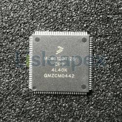
![MC9S12DT128]()
The MC9S12DT128 is a 16-bit microcontroller chip by Freescale (now NXP)
製造商: FREESCALE 包裝/箱: TQFP11
7,695 有存貨
貨物週期: 3~7 天
最小訂購量為 1
-
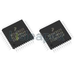
![MC56F8025V]()
7,729 有存貨
貨物週期: 3~7 天
最小訂購量為 1
-
![MC9S08GB60A]()
3,328 有存貨
貨物週期: 3~7 天
最小訂購量為 1
-
![MC68HC912D60A]()
MC68HC912D60A is a 16-bit microcontroller from Freescale, suitable for automotive and industrial applications.
製造商: FREESCALE 包裝/箱: QFP
1 有存貨
貨物週期: 3~7 天
最小訂購量為 1
-
![MC68HC912D60]()
MC68HC912D60 is a 16-bit microcontroller chip with 60KB flash memory and 2KB RAM for embedded systems.
製造商: FREESCALE 包裝/箱: QFP
3,454 有存貨
貨物週期: 3~7 天
最小訂購量為 1
-
![MCIMX6Q-SL]()
MCIMX6Q-SL is a low-power, single-core Cortex-A9 processor designed for industrial and automotive applications.
製造商: FREESCALE 包裝/箱: BGA
5,148 有存貨
貨物週期: 3~7 天
最小訂購量為 1
-
![MC68HC05B16]()
MC68HC05B16 is an 8-bit microcontroller with 16KB OTP ROM and 512 bytes RAM, manufactured by Motorola.
製造商: FREESCALE 包裝/箱: PLCC-52
6,655 有存貨
貨物週期: 3~7 天
最小訂購量為 1
-
![MC9S08AC96]()
MC9S08AC96 is a 8-bit microcontroller with 96 KB flash and 6 KB RAM, ideal for various applications.
製造商: FREESCALE 包裝/箱: QFP-44
4,883 有存貨
貨物週期: 3~7 天
最小訂購量為 1
-
![MC68HC908GT16]()
MC68HC908GT16 is a low-cost, high-performance 8-bit microcontroller with 16 KB flash memory and 512 bytes RAM.
製造商: FREESCALE 包裝/箱: QFP44
3,799 有存貨
貨物週期: 3~7 天
最小訂購量為 1
-
![MC68HC08AZ60A]()
MC68HC08AZ60A is a low-cost, high-performance 8-bit microcontroller with flash memory and EEPROM.
製造商: FREESCALE 包裝/箱: QFP-64
3,673 有存貨
貨物週期: 3~7 天
最小訂購量為 1
-
![MC68HC912DG128A]()
MC68HC912DG128A is a 16-bit microcontroller with 128KB flash memory, operating at 50 MHz.
製造商: FREESCALE 包裝/箱: QFP112
4,507 有存貨
貨物週期: 3~7 天
最小訂購量為 1