恭喜您提交成功
 提交失敗
提交失敗
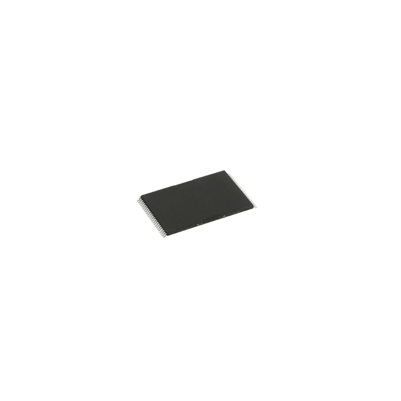
MBM29F040C-90PFTN
IC,EEPROM,NOR FLASH,512KX8,CMOS,TSSOP,32PIN,PLASTICMBM29F040C-90PFTN
IC,EEPROM,NOR FLASH,512KX8,CMOS,TSSOP,32PIN,PLASTIC
品質保證
品質保證
從我們的供應鍊網路採購的所有零件都經過嚴格的進貨檢驗流程。 這種細緻的檢查可確保客戶收到的零件是正品並符合要求的標準。 此外,我們還保存這些檢查的詳細記錄,以確保整個供應鏈的透明度和可追溯性。


認證
我們已成功獲得各項認證標準,並建立了自己的專業檢測實驗室。 這確保了我們向客戶提供的每件產品都符合最高的品質標準。 我們遵守嚴格的測試協議,以保持我們產品的一致性和準確性。 為了確保我們的產品是原裝正品,我們還與信譽良好的第三方檢測機構合作進行嚴格的品質測試。 我們對品質的承諾延伸到滿足行業、法律、監管和 ISO 9001:2015 的要求。
運輸與付款
運輸與付款
關於運送
我們通常會在幾個工作日內通過可靠的運輸公司(例如 FedEx、SF、UPS 或 DHL)運送訂單。 我們還支持其他運輸方式。 如果您想詢問具體的運輸細節或費用,請隨時與我們聯繫。


關於付款
我們接受多種支付方式,包括VISA、MasterCard、銀聯、西聯、PayPal等渠道。
如果您有特定的付款方式或想詢問費率和其他詳細信息,請隨時與我們聯繫。

電匯

Paypal

信用卡

西聯匯款

速匯金
服務與包裝
服務與包裝
About After Sales Service
All Parts Extended Quality Guarantee
自發貨之日起 90 天內發起申請。
與我們的工作人員確認退貨或換貨。
保持貨物收到時的原始狀態。
最後請注意,退貨或換貨的資格取決於對退貨商品實際狀況的評估。 在完成退貨或換貨流程之前,我們將評估收到的貨物。 如果您對退貨或換貨有任何疑問或需要進一步幫助,請隨時通過以下方式聯絡我們: [email protected]
關於包裝
在包裝方面,我們的產品均精心包裝在防靜電袋中,以提供ESD防靜電保護。 外包裝堅固耐用且閉合牢固。 我們支持各種包裝方法,例如捲帶式、切帶式、管式或託盤式。

例子

捲帶式

剪膠帶

管或託盤
MBM29F040C-90PFTN 數據表

目前的價格方案正在編制中。請聯絡我們的客戶服務團隊獲取最新的價格資訊。感謝您的理解和支援!
詳細說明
■ GENERAL DESCRIPTION The MBM29F040C is a 4M-bit, 5.0 V-only Flash memory organized as 512K bytes of 8 bits each. The MBM29F040C is offered in a 32-pin PLCC and 32-pin TSOP(I) package. This device is designed to be programmed in-system with the standard system 5.0 V VCCsupply. A 12.0 V VPPis not required for write or erase operations. The device can also be reprogrammed in standard EPROM programmers. ■ FEATURES • Single 5.0 V read, program and erase Minimizes system level power requirements • Compatible with JEDEC-standard commands Uses same software commands as E2PROMs • Compatible with JEDEC-standard byte-wide pinouts 32-pin PLCC (Package suffix: PD) 32-pin TSOP(I) (Package suffix: PF) 32-pin TSOP(I) (Package suffix: PFTN – Normal Bend Type, PFTR – Reversed Bend Type) • Minimum 100,000 write/erase cycles • High performance55 ns maximum access time • Sector erase architecture 8 equal size sectors of 64K bytes each Any combination of sectors can be concurrently erased. Also supports full chip erase. • Embedded Erase™ Algorithms Automatically pre-programs and erases the chip or any sector • Embedded Program™ Algorithms Automatically writes and verifies data at specified address • DataPolling and Toggle Bit feature for detection of program or erase cycle completion • Low VCCwrite inhibit ≤3.2 V • Sector protection Hardware method disables any combination of sectors from write or erase operations • Erase Suspend/Resume Suspends the erase operation to allow a read data in another sector within the same device

主要特徵
- Single 5.0 V read, program and erase Minimizes system level power requirements
- Compatible with JEDEC-standard commands Uses same software commands as E2PROMs
- Compatible with JEDEC-standard byte-wide pinouts
- 32-pin PLCC (Package suffix: PD)
- 32-pin TSOP(I) (Package suffix: PF)
- 32-pin TSOP(I) (Package suffix: PFTN – Normal Bend Type, PFTR – Reversed Bend Type)
- Minimum 100,000 write/erase cycles
- High performance
- 55 ns maximum access time
- Sector erase architecture
- 8 equal size sectors of 64K bytes each Any combination of sectors can be concurrently erased. Also supports full chip erase.
- Embedded Erase™ Algorithms
- Automatically pre-programs and erases the chip or any sector
- Embedded Program™ Algorithms
- Automatically writes and verifies data at specified address
- DataPolling and Toggle Bit feature for detection of program or erase cycle completion
- Low VCCwrite inhibit ≤3.2 V
- Sector protection
- Hardware method disables any combination of sectors from write or erase operations
- Erase Suspend/Resume
- Suspends the erase operation to allow a read data in another sector within the same device
規格
以下是所選零件的基本參數,涉及零件的特性及其所屬類別。
| Part Life Cycle Code | Active | Reach Compliance Code | compliant |
| Access Time-Max | 90 ns | Command User Interface | YES |
| Data Polling | YES | Endurance | 100000 Write/Erase Cycles |
| JESD-30 Code | R-PDSO-G32 | Memory Density | 4194304 bit |
| Memory IC Type | FLASH | Memory Width | 8 |
| Number of Sectors/Size | 8 | Number of Terminals | 32 |
| Number of Words | 524288 words | Number of Words Code | 512000 |
| Operating Temperature-Max | 85 °C | Operating Temperature-Min | -40 °C |
| Organization | 512KX8 | Package Body Material | PLASTIC/EPOXY |
| Package Code | TSSOP | Package Equivalence Code | TSSOP32,.8,20 |
| Package Shape | RECTANGULAR | Package Style | SMALL OUTLINE, THIN PROFILE, SHRINK PITCH |
| Parallel/Serial | PARALLEL | Power Supplies ! | 5 V |
| Qualification Status ! | Not Qualified | Sector Size | 64K |
| Standby Current-Max | 0.000005 A | Supply Current-Max | 0.045 mA |
| Supply Voltage-Nom (Vsup) | 5 V | Surface Mount ! | YES |
| Technology | CMOS | Temperature Grade ! | INDUSTRIAL |
| Terminal Form ! | GULL WING | Terminal Pitch ! | 0.5 mm |
| Terminal Position | DUAL | Toggle Bit | YES |
| Type | NOR TYPE |
數據表 PDF
數據表記錄了器件的特性、絕對最大額定值、應用等,這對於作為器件特定應用的整體指南大有裨益。
推薦零件
-
![MB90F543GSPF]()
3,718 有存貨
貨物週期: 3~7 天
最小訂購量為 1
-
![MB85R1001A]()
Memory Circuit, 128KX8, CMOS, PDSO48, 12 X 12.40 MM, 1.20 MM HEIGHT, 0.50 MM PITCH, PLASTIC, TSOP1-48
製造商: FUJITSU 包裝/箱: TSOP48
6,757 有存貨
貨物週期: 3~7 天
最小訂購量為 1