恭喜您提交成功
 提交失敗
提交失敗
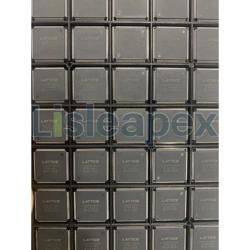
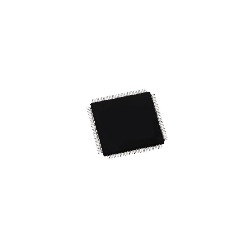
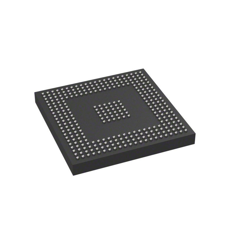
LCMXO2-4000HC-4TG144I
3.3V operating voltage and 4 Speed grades availableLCMXO2-4000HC-4TG144I
3.3V operating voltage and 4 Speed grades available
-
製造商零件號 # : LCMXO2-4000HC-4TG144I
-
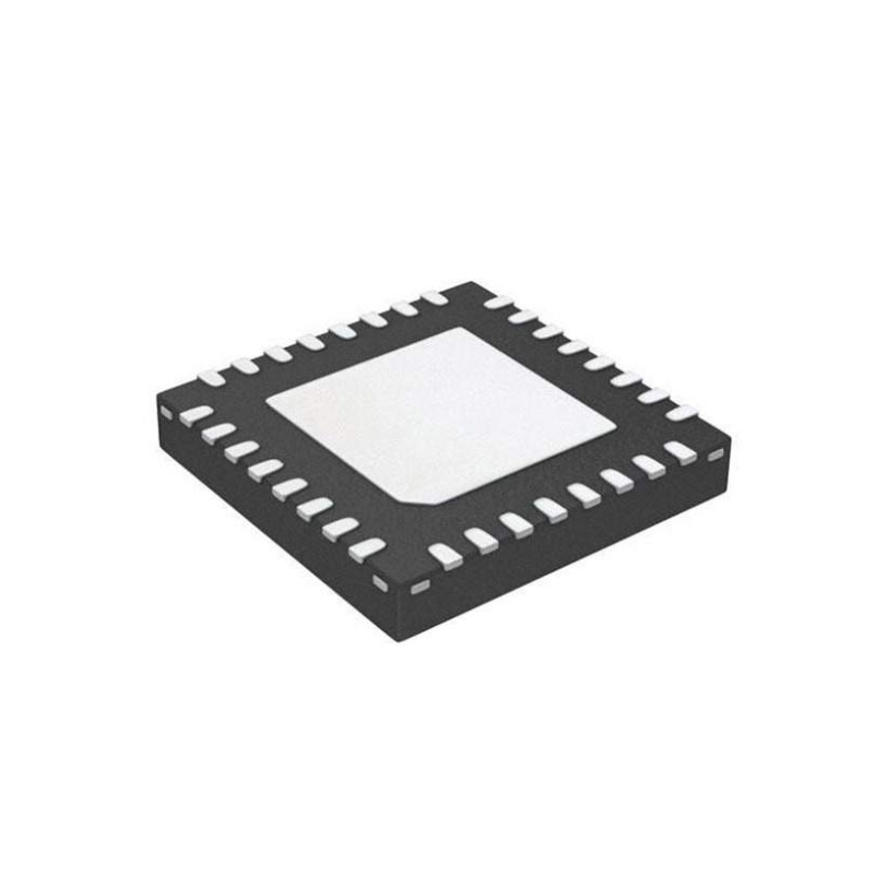
包裝/封裝: TQFP-144
-
產品分類 : FPGAs (Field Programmable Gate Array)
品質保證
品質保證
從我們的供應鍊網路採購的所有零件都經過嚴格的進貨檢驗流程。 這種細緻的檢查可確保客戶收到的零件是正品並符合要求的標準。 此外,我們還保存這些檢查的詳細記錄,以確保整個供應鏈的透明度和可追溯性。


認證
我們已成功獲得各項認證標準,並建立了自己的專業檢測實驗室。 這確保了我們向客戶提供的每件產品都符合最高的品質標準。 我們遵守嚴格的測試協議,以保持我們產品的一致性和準確性。 為了確保我們的產品是原裝正品,我們還與信譽良好的第三方檢測機構合作進行嚴格的品質測試。 我們對品質的承諾延伸到滿足行業、法律、監管和 ISO 9001:2015 的要求。
運輸與付款
運輸與付款
關於運送
我們通常會在幾個工作日內通過可靠的運輸公司(例如 FedEx、SF、UPS 或 DHL)運送訂單。 我們還支持其他運輸方式。 如果您想詢問具體的運輸細節或費用,請隨時與我們聯繫。


關於付款
我們接受多種支付方式,包括VISA、MasterCard、銀聯、西聯、PayPal等渠道。
如果您有特定的付款方式或想詢問費率和其他詳細信息,請隨時與我們聯繫。

電匯

Paypal

信用卡

西聯匯款

速匯金
服務與包裝
服務與包裝
About After Sales Service
All Parts Extended Quality Guarantee
自發貨之日起 90 天內發起申請。
與我們的工作人員確認退貨或換貨。
保持貨物收到時的原始狀態。
最後請注意,退貨或換貨的資格取決於對退貨商品實際狀況的評估。 在完成退貨或換貨流程之前,我們將評估收到的貨物。 如果您對退貨或換貨有任何疑問或需要進一步幫助,請隨時通過以下方式聯絡我們: [email protected]
關於包裝
在包裝方面,我們的產品均精心包裝在防靜電袋中,以提供ESD防靜電保護。 外包裝堅固耐用且閉合牢固。 我們支持各種包裝方法,例如捲帶式、切帶式、管式或託盤式。

例子

捲帶式

剪膠帶

管或託盤
LCMXO2-4000HC-4TG144I 數據表
價格 (USD)
| 數量 | 單價 | 總價 |
|---|---|---|
| 1 | $12.332 | $12.33 |
| 10 | $10.908 | $109.08 |
| 30 | $10.039 | $301.17 |
| 100 | $9.312 | $931.20 |
這些價格會受到市場波動的影響,需要提交報價才能取得最新價格。
詳細說明
The LCMXO2-4000HC-4TG144I is a powerful FPGA from Lattice Semiconductor, boasting 4000 LUTs and 4320 logic elements for extensive programmability. With 76 Kbits of embedded memory and 64 user I/Os, this FPGA offers versatility and performance. Its commercial temperature grade and 4x direct clock input structure ensure high-speed operation, while the 144-pin TQFP package allows for easy integration into diverse designs

主要特徵
- Flexible Logic Architecture
- Six devices with 256 to 6864 LUT4s and 19 to 335 I/Os
- Ultra Low Power Devices
- Advanced 65 nm low power process
- As low as 19 µW standby power
- Programmable low swing differential I/Os
- Stand-by mode and other power saving options
- Embedded and Distributed Memory
- Up to 240 Kbits sysMEM™ Embedded Block RAM
- Up to 54 Kbits Distributed RAM
- Dedicated FIFO control logic On-Chip User Flash Memory
- Up to 256 Kbits of User Flash Memory
- 100,000 write cycles
- Accessible through WISHBONE, SPI, I2C and JTAG interfaces
- Can be used as soft processor PROM or as Flash memory
- Pre-Engineered Source Synchronous I/O
- DDR registers in I/O cells
- Dedicated gearing logic
- 7:1 Gearing for Display I/Os
- Generic DDR, DDRX2, DDRX4
- Dedicated DDR/DDR2/LPDDR memory with DQS support
- High Performance, Flexible I/O Buffer
- Programmable sysIO™ buffer supports wide range of interfaces:
- – LVCMOS 3.3/2.5/1.8/1.5/1.2
- – LVTTL
- –PCI
- – LVDS, Bus-LVDS, MLVDS, RSDS, LVPECL
- – SSTL 25/18
- – HSTL 18
- – Schmitt trigger inputs, up to 0.5V hysteresis
- I/Os support hot socketing
- On-chip differential termination
- Programmable pull-up or pull-down mode

規格
以下是所選零件的基本參數,涉及零件的特性及其所屬類別。
| Product Category ! | FPGA - Field Programmable Gate Array | RoHS | Details |
| Series | LCMXO2 | Number of Logic Elements | 4320 LE |
| Adaptive Logic Modules - ALMs | 2160 ALM | Embedded Memory | 92 kbit |
| Number of I/Os | 114 I/O | Supply Voltage - Min | 2.375 V |
| Supply Voltage - Max | 3.6 V | Minimum Operating Temperature | - 40 C |
| Maximum Operating Temperature ! | + 100 C | Mounting Style | SMD/SMT |
| Package / Case | TQFP-144 | Brand | Lattice |
| Distributed RAM | 34 kbit | Embedded Block RAM - EBR | 92 kbit |
| Maximum Operating Frequency | 269 MHz | Moisture Sensitive | Yes |
| Number of Logic Array Blocks - LABs | 540 LAB | Operating Supply Current | 128 uA |
| Operating Supply Voltage ! | 2.5 V/3.3 V | Product Type ! | FPGA - Field Programmable Gate Array |
| Factory Pack Quantity | 60 | Subcategory | Programmable Logic ICs |
| Total Memory | 222 kbit | Tradename | MachXO2 |
| Unit Weight | 0.046530 oz |
Specification Comparison
數據表 PDF
數據表記錄了器件的特性、絕對最大額定值、應用等,這對於作為器件特定應用的整體指南大有裨益。
常見問題解答
What is LCMXO2-4000HC-4TG144I?
The LCMXO2-4000HC-4TG144I is a low-cost, low-power, instant-on non-volatile MachXO2 FPGA (Field-Programmable Gate Array) designed by Lattice Semiconductor. It is ideal for applications requiring programmable logic, such as consumer electronics, industrial automation, and communications systems.
How Does LCMXO2-4000HC-4TG144I Work?
The LCMXO2-4000HC-4TG144I works by allowing users to program the internal logic and interconnects to implement custom digital functions. This flexibility enables designers to create custom logic functions, signal processing algorithms, and interface protocols according to the specific requirements of their application.
How Many Pins does LCMXO2-4000HC-4TG144I have and What are the Functions of the Pinout Configuration?
The LCMXO2-4000HC-4TG144I is housed in a 144-pin TQFP (Thin Quad Flat Package) package. The pinout configuration includes:
- I/O Pins: Used for input and output of digital signals.
- Configuration Pins: Used for device configuration and initialization.
- Power Supply and Ground Pins: Provide the necessary voltage and ground connections for the device.
- Programming Pins: Used for in-system programming and configuration of the FPGA.
What are the Pros and Cons of LCMXO2-4000HC-4TG144I?
Pros:
- Low Cost: Provides cost-effective programmable logic for various applications.
- Low Power Consumption: Operates with low power requirements, suitable for battery-powered devices.
- Instant-On Feature: Enables rapid initialization and configuration for quick system startup.
- Non-Volatile Configuration: Retains the programmed configuration even when powered off.
- Flexible Logic Implementation: Allows custom digital functions and algorithms to be implemented as per specific application needs.
Cons:
- Resource Limitations: May have limited resources compared to larger FPGAs for complex designs.
- Routing Constraints: Design complexity may be limited by the available routing resources.
- Programming Overheads: Device programming and configuration may require additional time and considerations.
Are There Any Equivalents/Alternatives to LCMXO2-4000HC-4TG144I for Recommendation?
- The ICE40HX1K from Lattice Semiconductor is a low-cost alternative with a smaller logic capacity.
- Similar alternatives to the LCMXO2-4000HC-4TG144I include the EPM240T100C5N from Intel and the ATF1502ASV from Microchip Technology.
推薦零件
-
![PALCE16V8H-25PC/4]()
PALCE16V8H-25PC/4 is a versatile SPLD from the PAL family
製造商: Lattice 包裝/箱: PDIP-20
7,898 有存貨
貨物週期: 3~7 天
最小訂購量為 1
-
![LC4128V-75TN100C]()
7,609 有存貨
貨物週期: 3~7 天
最小訂購量為 1
-
![LCMXO2-640HC-4TG100I]()
4,302 有存貨
貨物週期: 3~7 天
最小訂購量為 1
-
![LCMXO1200C-3TN144C]()
LCMXO1200C-3TN144C
$7.639 Leverage its extensive logic resources and advanced memory capabilities for next-generation designs
製造商: LATTICE 包裝/箱: TQFP-144
5,466 有存貨
貨物週期: 3~7 天
最小訂購量為 1
-
![LCMXO2-1200HC-4SG32C]()
High-Speed, Low-Voltage EP Tray Solution for Industrial Automatio
製造商: Lattice 包裝/箱: QFN-32
4,889 有存貨
貨物週期: 3~7 天
最小訂購量為 1
-
![PALCE22V10H-15PC/4]()
4,626 有存貨
貨物週期: 3~7 天
最小訂購量為 1
-
![LC4256ZE-5TN144C]()
4,096 有存貨
貨物週期: 3~7 天
最小訂購量為 1
-
![LC4256ZE-7TN144I]()
LC4256ZE-7TN144I
$8.953 Complex Programmable Logic Devices with 96 I/O
製造商: Lattice Semiconductor 包裝/箱: QFP-144
7,810 有存貨
貨物週期: 3~7 天
最小訂購量為 1
-
![LCMXO2-256HC-4SG32I]()
6,501 有存貨
貨物週期: 3~7 天
最小訂購量為 1
-
![LCMXO2-256HC-4SG48C]()
LCMXO2-256HC-4SG48C
$1.598 Versatile Programmable Logic Device
製造商: Lattice Semiconductor 包裝/箱: QFN-48
5,977 有存貨
貨物週期: 3~7 天
最小訂購量為 1
-
![LCMXO3LF-4300C-6BG256I]()
LCMXO3LF-4300C-6BG256I is an FPGA with 4320 LUTs
製造商: Lattice Semiconductor 包裝/箱: CSFBGA-256
7,425 有存貨
貨物週期: 3~7 天
最小訂購量為 1
-
![LCMXO3LF-6900C-6BG400I]()
4,616 有存貨
貨物週期: 3~7 天
最小訂購量為 1
-
![LCMXO3LF-2100E-5MG256C]()
5,381 有存貨
貨物週期: 3~7 天
最小訂購量為 1
-
![LCMXO3LF-6900C-5BG256C]()
LCMXO3LF-6900C-5BG256C
$6.583 6864 858 CABGA-256 LCMXO3LF-6900C-5BG256C Programmable Logic Device (CPLDs/FPGAs) ROHS
製造商: Lattice Semiconductor 包裝/箱: CSFBGA-256
4,364 有存貨
貨物週期: 3~7 天
最小訂購量為 1
-
![LCMXO3LF-4300C-5BG324C]()
LCMXO3LF-4300C-5BG324C
$6.114 The 4320 LUTs in the LCMXO3LF-4300C-5BG324C make it a powerful Field Programmable Gate Array
製造商: LATTICE 包裝/箱: 324-LFBGA
6,871 有存貨
貨物週期: 3~7 天
最小訂購量為 1
-
![LCMXO2-640HC-4SG48I]()
Low-power consumption, ideal for various applications
製造商: Lattice Semiconductor 包裝/箱: QFN-48
5,155 有存貨
貨物週期: 3~7 天
最小訂購量為 1