恭喜您提交成功
 提交失敗
提交失敗
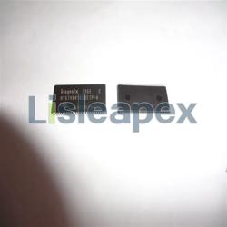
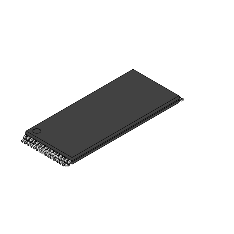
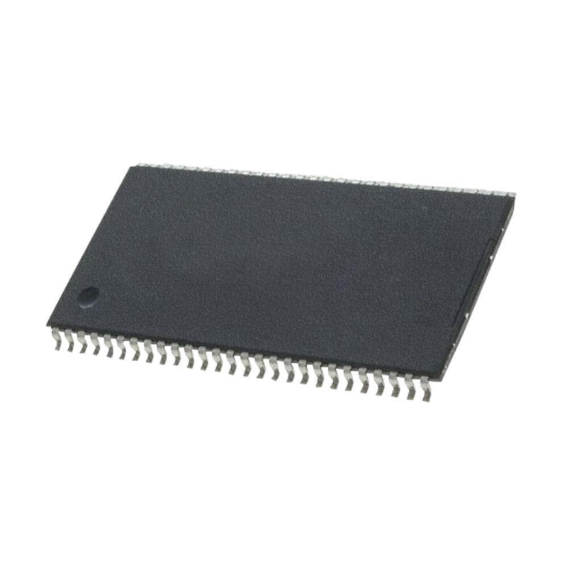
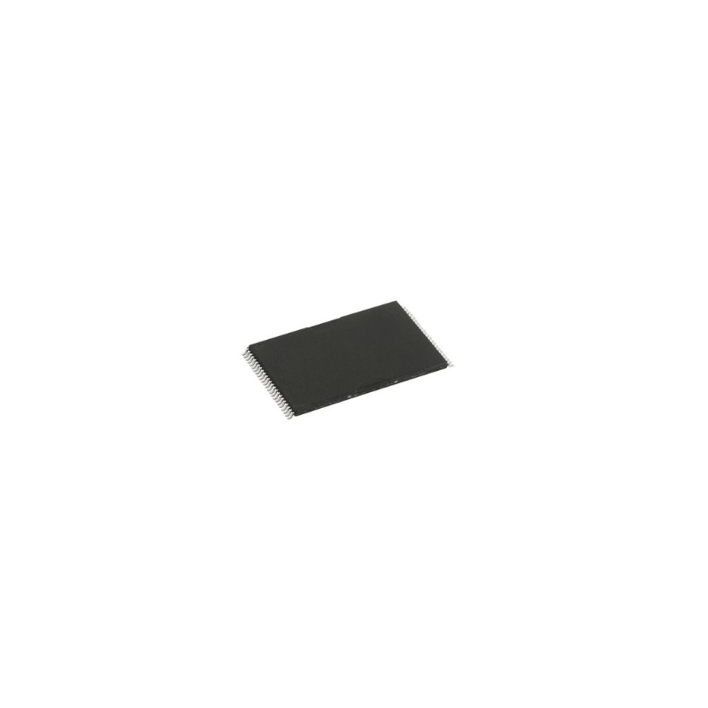
HY5DU121622CTP-D43
DDR DRAM, 32MX16, 0.7ns, CMOS, PDSO66, 0.400 X 0.875 INCH, 0.65 PITCH, ROHS COMPLIANT, TSOP2-66HY5DU121622CTP-D43
DDR DRAM, 32MX16, 0.7ns, CMOS, PDSO66, 0.400 X 0.875 INCH, 0.65 PITCH, ROHS COMPLIANT, TSOP2-66
品質保證
品質保證
從我們的供應鍊網路採購的所有零件都經過嚴格的進貨檢驗流程。 這種細緻的檢查可確保客戶收到的零件是正品並符合要求的標準。 此外,我們還保存這些檢查的詳細記錄,以確保整個供應鏈的透明度和可追溯性。


認證
我們已成功獲得各項認證標準,並建立了自己的專業檢測實驗室。 這確保了我們向客戶提供的每件產品都符合最高的品質標準。 我們遵守嚴格的測試協議,以保持我們產品的一致性和準確性。 為了確保我們的產品是原裝正品,我們還與信譽良好的第三方檢測機構合作進行嚴格的品質測試。 我們對品質的承諾延伸到滿足行業、法律、監管和 ISO 9001:2015 的要求。
運輸與付款
運輸與付款
關於運送
我們通常會在幾個工作日內通過可靠的運輸公司(例如 FedEx、SF、UPS 或 DHL)運送訂單。 我們還支持其他運輸方式。 如果您想詢問具體的運輸細節或費用,請隨時與我們聯繫。


關於付款
我們接受多種支付方式,包括VISA、MasterCard、銀聯、西聯、PayPal等渠道。
如果您有特定的付款方式或想詢問費率和其他詳細信息,請隨時與我們聯繫。

電匯

Paypal

信用卡

西聯匯款

速匯金
服務與包裝
服務與包裝
About After Sales Service
All Parts Extended Quality Guarantee
自發貨之日起 90 天內發起申請。
與我們的工作人員確認退貨或換貨。
保持貨物收到時的原始狀態。
最後請注意,退貨或換貨的資格取決於對退貨商品實際狀況的評估。 在完成退貨或換貨流程之前,我們將評估收到的貨物。 如果您對退貨或換貨有任何疑問或需要進一步幫助,請隨時通過以下方式聯絡我們: [email protected]
關於包裝
在包裝方面,我們的產品均精心包裝在防靜電袋中,以提供ESD防靜電保護。 外包裝堅固耐用且閉合牢固。 我們支持各種包裝方法,例如捲帶式、切帶式、管式或託盤式。

例子

捲帶式

剪膠帶

管或託盤
HY5DU121622CTP-D43 數據表

目前的價格方案正在編制中。請聯絡我們的客戶服務團隊獲取最新的價格資訊。感謝您的理解和支援!
詳細說明
The Hynix HY5DV641622 is a 67,108,864-bit CMOS Double Data Rate(DDR) Synchronous DRAM, ideally suited for the point-to-point applications which requires high bandwidth.FEATURES •3.3V for VDDand 2.5V for VDDQpower supply • All inputs and outputs are compatible with SSTL_2 interface • JEDEC standard 400mil 66pin TSOP-II with 0.65mm pin pitch • Fully differential clock inputs (CK, /CK) operation • Double data rate interface • Source synchronous - data transaction aligned to bidirectional data strobe (DQS) • x16 device has 2 bytewide data strobes (LDQS, UDQS) per each x8 I/O • Data outputs on DQS edges when read (edged DQ) Data inputs on DQS centers when write (centered DQ) • Data(DQ) and Write masks(DM) latched on the both rising and falling edges of the data strobe • All addresses and control inputs except Data, Data strobes and Data masks latched on the rising edges of the clock • Write mask byte controls by LDM and UDM • Programmable /CAS Latency 3 / 4 supported • Programmable Burst Length 2 / 4 / 8 with both sequential and interleave mode • Internal 4 bank operations with single pulsed /RAS • tRAS Lock-Out function supported • Auto refresh and self refresh supported • 4096 refresh cycles / 64ms • Full, Half and Matched Impedance(Weak) strength driver option controlled by EMRS

主要特徵
- 3.3V for VDDand 2.5V for VDDQpower supply
- All inputs and outputs are compatible with SSTL_2 interface
- JEDEC standard 400mil 66pin TSOP-II with 0.65mm pin pitch
- Fully differential clock inputs (CK, /CK) operation
- Double data rate interface
- Source synchronous - data transaction aligned to bidirectional data strobe (DQS)
- x16 device has 2 bytewide data strobes (LDQS, UDQS) per each x8 I/O
- Data outputs on DQS edges when read (edged DQ) Data inputs on DQS centers when write (centered DQ)
- Data(DQ) and Write masks(DM) latched on the both rising and falling edges of the data strobe
- All addresses and control inputs except Data, Data strobes and Data masks latched on the rising edges of the clock
- Write mask byte controls by LDM and UDM
- Programmable /CAS Latency 3 / 4 supported
- Programmable Burst Length 2 / 4 / 8 with both sequential and interleave mode
- Internal 4 bank operations with single pulsed /RAS
- tRAS Lock-Out function supported
- Auto refresh and self refresh supported
- 4096 refresh cycles / 64ms
- Full, Half and Matched Impedance(Weak) strength driver option controlled by EMRS
規格
以下是所選零件的基本參數,涉及零件的特性及其所屬類別。
| Pbfree Code | Yes | Rohs Code | Yes |
| Part Life Cycle Code | Obsolete | Part Package Code | TSOP2 |
| Pin Count ! | 66 | Reach Compliance Code | |
| ECCN Code | EAR99 | HTS Code ! | 8542.32.00.28 |
| Access Mode ! | FOUR BANK PAGE BURST | Access Time-Max | 0.7 ns |
| Additional Feature ! | AUTO/SELF REFRESH | Clock Frequency-Max (fCLK) | 200 MHz |
| I/O Type | COMMON | Interleaved Burst Length | 2,4,8 |
| JESD-30 Code | R-PDSO-G66 | JESD-609 Code | e6 |
| Length | 22.225 mm | Memory Density | 536870912 bit |
| Memory IC Type | DDR1 DRAM | Memory Width | 16 |
| Number of Functions | 1 | Number of Ports ! | 1 |
| Number of Terminals | 66 | Number of Words | 33554432 words |
| Number of Words Code | 32000000 | Operating Mode ! | SYNCHRONOUS |
| Operating Temperature-Max | 70 °C | Operating Temperature-Min | |
| Organization | 32MX16 | Output Characteristics | 3-STATE |
| Package Body Material | PLASTIC/EPOXY | Package Code | TSOP2 |
| Package Equivalence Code | TSSOP66,.46 | Package Shape | RECTANGULAR |
| Package Style | SMALL OUTLINE, THIN PROFILE | Power Supplies ! | 2.6 V |
| Qualification Status ! | Not Qualified | Refresh Cycles | 8192 |
| Seated Height-Max | 1.194 mm | Self Refresh | YES |
| Sequential Burst Length | 2,4,8 | Standby Current-Max | 0.01 A |
| Supply Voltage-Max (Vsup) | 2.7 V | Supply Voltage-Min (Vsup) | 2.5 V |
| Supply Voltage-Nom (Vsup) | 2.6 V | Surface Mount ! | YES |
| Technology | CMOS | Temperature Grade ! | COMMERCIAL |
| Terminal Finish | TIN BISMUTH | Terminal Form ! | GULL WING |
| Terminal Pitch ! | 0.65 mm | Terminal Position | DUAL |
| Width | 10.16 mm |
Specification Comparison
數據表 PDF
數據表記錄了器件的特性、絕對最大額定值、應用等,這對於作為器件特定應用的整體指南大有裨益。
常見問題解答
What is HY5DU121622CTP-D43?
The HY5DU121622CTP-D43 is a 512Mb Double Data Rate 2 (DDR2) Synchronous Dynamic Random Access Memory (SDRAM) chip designed by SK Hynix. It is commonly used in computing systems, networking equipment, and consumer electronics for high-speed data storage and retrieval.
How Does HY5DU121622CTP-D43 Work?
The HY5DU121622CTP-D43 works by storing and retrieving digital data with high speed and efficiency. It utilizes double data rate architecture to transfer data on both the rising and falling edges of the clock signal, effectively doubling the data transfer rate. The SDRAM chip is synchronized with the system clock to ensure accurate and timely data operations.
How Many Pins does HY5DU121622CTP-D43 have and What are the Functions of the Pinout Configuration?
The HY5DU121622CTP-D43 is housed in a 84-ball FBGA (Fine-pitch Ball Grid Array) package. The pinout configuration includes:
- VDD, VDDQ: Power supply pins for core and I/O, respectively.
- VSS, VSSQ: Ground pins for core and I/O, respectively.
- DQ, DM: Data input/output and data mask pins.
- CLK, /CLK: Clock input and its complement.
- CS, /CS: Chip select input and its complement.
- WE, /CAS, /RAS: Write enable, column address strobe, and row address strobe inputs.
- BA0-BA2: Bank address inputs.
- ODT: On-die termination control.
What are the Pros and Cons of HY5DU121622CTP-D43?
Pros:
- High-Speed Operation: Provides high-speed data transfer suitable for demanding applications.
- Double Data Rate: Utilizes DDR2 architecture for efficient data transfer on both clock edges.
- Large Capacity: Offers 512Mb storage capacity for storing significant amounts of data.
- Synchronous Interface: Synchronizes with the system clock for accurate and reliable operation.
- Compact Form Factor: The FBGA package allows for space-efficient placement on PCBs.
Cons:
- Component Matching: Requires careful PCB layout and signal integrity considerations for optimal performance.
- Complex Initialization: DDR2 SDRAM initialization sequence may be more complex compared to older SDRAM types.
- Power Consumption: Higher speed operation may result in relatively higher power consumption.
Are There Any Equivalents/Alternatives to HY5DU121622CTP-D43 for Recommendation?
- The MT47H64M16HR-3 from Micron Technology is a comparable DDR2 SDRAM chip with similar specifications.
- Possible alternatives to the HY5DU121622CTP-D43 include the K4T51163QJ-BCE7 from Samsung and the H5PS5162GFR-S6C from SK Hynix.
推薦零件
-
![HY5PS121621CFP-Y5]()
6,959 有存貨
貨物週期: 3~7 天
最小訂購量為 1
-
![HY27UF084G2M-TPCB]()
Flash, 512MX8, 25ns, PDSO48, 12 X 20 MM, 1.20 MM HEIGHT, LEAD FREE, PLASTIC, TSOP1-48
製造商: HYNIX 包裝/箱: TSOP-48
4,676 有存貨
貨物週期: 3~7 天
最小訂購量為 1
-
![HY27UF084G2B]()
7,411 有存貨
貨物週期: 3~7 天
最小訂購量為 1
-
![HY5PS12821C]()
HY5PS12821C is a high-performance, low-power DDR2 SDRAM chip for various applications.
製造商: HYNIX 包裝/箱: BGA
5,179 有存貨
貨物週期: 3~7 天
最小訂購量為 1
-
![HY5PS1G431C]()
High performance 1Gb mobile SD RAM chip for smartphones and tablets.
製造商: HYNIX 包裝/箱: BULKBGA
3,621 有存貨
貨物週期: 3~7 天
最小訂購量為 1
-
![HY5PS1G1631CFP-S6]()
7,143 有存貨
貨物週期: 3~7 天
最小訂購量為 1
-
![HY27UU088G5M]()
6,404 有存貨
貨物週期: 3~7 天
最小訂購量為 1
-
![HY5PS12821B]()
HY5PS12821B is a DDR2 SDRAM chip with 128MB capacity and operates at 800MHz speed.
製造商: HYNIX 包裝/箱: BGA
3,660 有存貨
貨物週期: 3~7 天
最小訂購量為 1
-
![HY5RS123235BFP-14]()
DDR DRAM 16MX32 with 0.26NS speed, CMOS technology in PBGA136 package
製造商: HYNIX 包裝/箱: BGA
4,243 有存貨
貨物週期: 3~7 天
最小訂購量為 1
-
![HY27UF081G2A]()
HY27UF081G2A is a high-performance, low-power NAND Flash memory chip commonly used in electronic devices.
製造商: HYNIX 包裝/箱: TSOP-48
5,735 有存貨
貨物週期: 3~7 天
最小訂購量為 1
-
![HY57V161610ETP]()
HY57V161610ETP is a 16Mb Synchronous DRAM chip with a data transfer rate of 143MHz.
製造商: HYNIX 包裝/箱: TSSOP
3,534 有存貨
貨物週期: 3~7 天
最小訂購量為 1
-
![HY27US08121B]()
HY27US08121B is a high-performance 8Gb NAND Flash memory chip with 2.7-3.6V voltage.
製造商: HYNIX 包裝/箱: TSOP48
3,616 有存貨
貨物週期: 3~7 天
最小訂購量為 1
-
![HY57V658020]()
HY57V658020 is a 256Mb Synchronous DRAM chip for high-speed memory applications.
製造商: HYNIX 包裝/箱: TSSOP5
6,697 有存貨
貨物週期: 3~7 天
最小訂購量為 1