恭喜您提交成功
 提交失敗
提交失敗
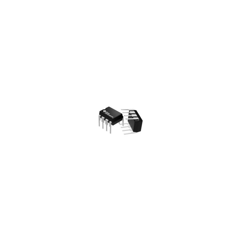
HEF4023BP
The HEF4023BP is a triple 3-input NAND gate in a PDIP14 package, belonging to the 4000/14000/40000 series
HEF4023BP
The HEF4023BP is a triple 3-input NAND gate in a PDIP14 package, belonging to the 4000/14000/40000 series
品質保證
品質保證
從我們的供應鍊網路採購的所有零件都經過嚴格的進貨檢驗流程。 這種細緻的檢查可確保客戶收到的零件是正品並符合要求的標準。 此外,我們還保存這些檢查的詳細記錄,以確保整個供應鏈的透明度和可追溯性。


認證
我們已成功獲得各項認證標準,並建立了自己的專業檢測實驗室。 這確保了我們向客戶提供的每件產品都符合最高的品質標準。 我們遵守嚴格的測試協議,以保持我們產品的一致性和準確性。 為了確保我們的產品是原裝正品,我們還與信譽良好的第三方檢測機構合作進行嚴格的品質測試。 我們對品質的承諾延伸到滿足行業、法律、監管和 ISO 9001:2015 的要求。
運輸與付款
運輸與付款
關於運送
我們通常會在幾個工作日內通過可靠的運輸公司(例如 FedEx、SF、UPS 或 DHL)運送訂單。 我們還支持其他運輸方式。 如果您想詢問具體的運輸細節或費用,請隨時與我們聯繫。


關於付款
我們接受多種支付方式,包括VISA、MasterCard、銀聯、西聯、PayPal等渠道。
如果您有特定的付款方式或想詢問費率和其他詳細信息,請隨時與我們聯繫。

電匯

Paypal

信用卡

西聯匯款

速匯金
服務與包裝
服務與包裝
About After Sales Service
All Parts Extended Quality Guarantee
自發貨之日起 90 天內發起申請。
與我們的工作人員確認退貨或換貨。
保持貨物收到時的原始狀態。
最後請注意,退貨或換貨的資格取決於對退貨商品實際狀況的評估。 在完成退貨或換貨流程之前,我們將評估收到的貨物。 如果您對退貨或換貨有任何疑問或需要進一步幫助,請隨時通過以下方式聯絡我們: [email protected]
關於包裝
在包裝方面,我們的產品均精心包裝在防靜電袋中,以提供ESD防靜電保護。 外包裝堅固耐用且閉合牢固。 我們支持各種包裝方法,例如捲帶式、切帶式、管式或託盤式。

例子

捲帶式

剪膠帶

管或託盤
HEF4023BP 數據表

目前的價格方案正在編制中。請聯絡我們的客戶服務團隊獲取最新的價格資訊。感謝您的理解和支援!
詳細說明
The HEF4023BP is a high-speed CMOS quad 3-input NAND gate with 5V supply voltage. It is part of the HEF4000B series of integrated circuits, which are designed for use in a wide range of applications including industrial, automotive, consumer electronics, and telecommunications.This device features four independent 3-input NAND gates, each with its own output. The inputs are buffered to ensure a stable operation and are compatible with standard TTL inputs. The output stage is capable of driving up to 10 standard TTL loads, making it suitable for use in a variety of digital logic applications.The HEF4023BP operates over a wide temperature range from -40°C to 125°C, making it suitable for use in harsh environments. It is available in a 14-pin DIP package, making it easy to integrate into existing circuit designs.
主要特徵
- Quad 2-input NAND gate
- Operating voltage range: 3V to 20V
- Output current: ±6mA
- Operating temperature range: -40°C to 85°C
- High noise immunity: 0.45 V
- Low power consumption: 40µW
- Wide supply voltage range: 3V to 20V
應用
- Industrial control systems
- Automotive electronics
- Home automation
- Consumer electronics
- Communication equipment
- Medical devices
- Robotics
- Instrumentation
- Sensor interfacing
規格
以下是所選零件的基本參數,涉及零件的特性及其所屬類別。
| Manufacturer | NXP Semiconductors | Product Category ! | Gates and Inverters |
數據表 PDF
數據表記錄了器件的特性、絕對最大額定值、應用等,這對於作為器件特定應用的整體指南大有裨益。
常見問題解答
What is HEF4023BP?
The HEF4023BP is a triple 3-input NAND gate integrated circuit (IC) manufactured by NXP Semiconductors. It is commonly used in digital logic applications for combining multiple input signals and producing a single output based on the NAND gate logic function.
How Does HEF4023BP Work?
The HEF4023BP operates by accepting three input signals and performing a logical AND operation on them through its internal NAND gates. The output of the NAND gates reflects the result of the logical operation, making it suitable for applications that require complex combinational logic functions.
How Many Pins does HEF4023BP have and What are the Functions of the Pinout Configuration?
The HEF4023BP is housed in a 14-pin DIP (Dual Inline Package) package. The pinout configuration includes:
- 1A, 2A, 3A: Inputs for the first, second, and third NAND gates.
- 1B, 2B, 3B: Inputs for the first, second, and third NAND gates.
- 1Y, 2Y, 3Y: Outputs of the first, second, and third NAND gates.
- VCC: Positive power supply pin.
- GND: Ground pin.
What are the Pros and Cons of HEF4023BP?
Pros:
- High Integration: Combines three 3-input NAND gates in a single IC, saving board space and reducing component count.
- Wide Operating Voltage Range: Supports a wide range of supply voltages, enhancing flexibility in different applications.
- Simple Logic Function: Performs the NAND gate function, suitable for various logic operations and signal processing tasks.
- Standard Package: Housed in a widely used 14-pin DIP package for easy integration into electronic designs.
Cons:
- Non-Inverting Outputs: The outputs are not inverted, which may require additional components for specific logic functions.
- Power Consumption: May consume more power compared to specialized, low-power logic gates in certain applications.
Are There Any Equivalents/Alternatives to HEF4023BP for Recommendation?
An equivalent part to the HEF4023BP is the CD4023B from Texas Instruments. Alternatives to the HEF4023BP include the MC14023B from ON Semiconductor and the SN74HC10 from Texas Instruments.
推薦零件
-
![PCF8582C-2]()
4,240 有存貨
貨物週期: 3~7 天
最小訂購量為 1
-
![PCF8594C-2]()
The PCF8594C-2 is a 8-bit I2C-bus I/O expander for efficient communication with multiple peripherals
製造商: PHILIPS 包裝/箱: SOP8
7,529 有存貨
貨物週期: 3~7 天
最小訂購量為 1