恭喜您提交成功
 提交失敗
提交失敗
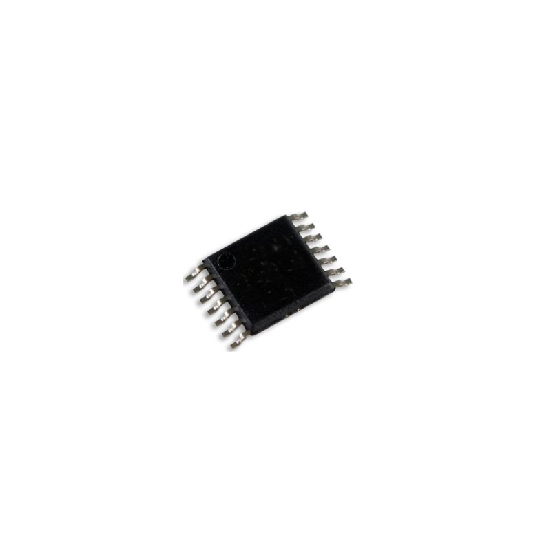
DM74S74N
With its advanced logic design, this integrated circuit provides precise timing and accurate data transfer in complex digital system
DM74S74N
With its advanced logic design, this integrated circuit provides precise timing and accurate data transfer in complex digital system
品質保證
品質保證
從我們的供應鍊網路採購的所有零件都經過嚴格的進貨檢驗流程。 這種細緻的檢查可確保客戶收到的零件是正品並符合要求的標準。 此外,我們還保存這些檢查的詳細記錄,以確保整個供應鏈的透明度和可追溯性。


認證
我們已成功獲得各項認證標準,並建立了自己的專業檢測實驗室。 這確保了我們向客戶提供的每件產品都符合最高的品質標準。 我們遵守嚴格的測試協議,以保持我們產品的一致性和準確性。 為了確保我們的產品是原裝正品,我們還與信譽良好的第三方檢測機構合作進行嚴格的品質測試。 我們對品質的承諾延伸到滿足行業、法律、監管和 ISO 9001:2015 的要求。
運輸與付款
運輸與付款
關於運送
我們通常會在幾個工作日內通過可靠的運輸公司(例如 FedEx、SF、UPS 或 DHL)運送訂單。 我們還支持其他運輸方式。 如果您想詢問具體的運輸細節或費用,請隨時與我們聯繫。


關於付款
我們接受多種支付方式,包括VISA、MasterCard、銀聯、西聯、PayPal等渠道。
如果您有特定的付款方式或想詢問費率和其他詳細信息,請隨時與我們聯繫。

電匯

Paypal

信用卡

西聯匯款

速匯金
服務與包裝
服務與包裝
About After Sales Service
All Parts Extended Quality Guarantee
自發貨之日起 90 天內發起申請。
與我們的工作人員確認退貨或換貨。
保持貨物收到時的原始狀態。
最後請注意,退貨或換貨的資格取決於對退貨商品實際狀況的評估。 在完成退貨或換貨流程之前,我們將評估收到的貨物。 如果您對退貨或換貨有任何疑問或需要進一步幫助,請隨時通過以下方式聯絡我們: [email protected]
關於包裝
在包裝方面,我們的產品均精心包裝在防靜電袋中,以提供ESD防靜電保護。 外包裝堅固耐用且閉合牢固。 我們支持各種包裝方法,例如捲帶式、切帶式、管式或託盤式。

例子

捲帶式

剪膠帶

管或託盤
DM74S74N 數據表
價格 (USD)
| 數量 | 單價 | 總價 |
|---|---|---|
| 1 | $0.167 | $0.17 |
| 200 | $0.064 | $12.80 |
| 500 | $0.062 | $31.00 |
| 1000 | $0.061 | $61.00 |
這些價格會受到市場波動的影響,需要提交報價才能取得最新價格。
詳細說明
General Description This device contains two independent positive-edge-triggered D flip-flops with complementary outputs. The information on the D input is accepted by the flip-flops on the positive going edge of the clock pulse. The triggering occurs at a voltage level and is not directly related to the transition time of the rising edge of the clock. The data on the D input may be changed while the clock is LOW or HIGH without affecting the outputs as long as setup and hold times are not violated. A low logic level on the preset or clear inputs will set or reset the outputs regardless of the logic levels of the other inputs.
規格
以下是所選零件的基本參數,涉及零件的特性及其所屬類別。
| Part Life Cycle Code | Contact Manufacturer | Part Package Code | DIP |
| Pin Count ! | 14 | Reach Compliance Code | |
| HTS Code ! | 8542.39.00.01 | Family | S |
| JESD-30 Code | R-PDIP-T14 | Length | 19.18 mm |
| Logic IC Type | D FLIP-FLOP | Number of Bits | 1 |
| Number of Functions | 2 | Number of Terminals | 14 |
| Operating Temperature-Max | 70 °C | Operating Temperature-Min | |
| Output Polarity | COMPLEMENTARY | Package Body Material | PLASTIC/EPOXY |
| Package Code | DIP | Package Shape | RECTANGULAR |
| Package Style | IN-LINE | Propagation Delay (tpd) | 14 ns |
| Qualification Status ! | Not Qualified | Seated Height-Max | 5.08 mm |
| Supply Voltage-Max (Vsup) | 5.25 V | Supply Voltage-Min (Vsup) | 4.75 V |
| Supply Voltage-Nom (Vsup) | 5 V | Surface Mount ! | NO |
| Technology | TTL | Temperature Grade ! | COMMERCIAL |
| Terminal Form ! | THROUGH-HOLE | Terminal Pitch ! | 2.54 mm |
| Terminal Position | DUAL | Trigger Type | POSITIVE EDGE |
| Width | 7.62 mm | fmax-Min | 110 MHz |
| Series | 74S | Package | Tube |
| Product Status | Obsolete | Function | Set(Preset) and Reset |
| Type | D-Type | Output Type | Complementary |
| Number of Elements | 2 | Number of Bits per Element | 1 |
| Clock Frequency | 65 MHz | Current - Output High, Low | 1mA, 20mA |
| Voltage - Supply | 4.75V ~ 5.25V | Operating Temperature ! | 0°C ~ 70°C (TA) |
| Mounting Type | Through Hole | Supplier Device Package | 14-DIP |
| Package / Case | 14-DIP (0.300", 7.62mm) | Base Product Number | 74S74 |
數據表 PDF
數據表記錄了器件的特性、絕對最大額定值、應用等,這對於作為器件特定應用的整體指南大有裨益。
常見問題解答
What is DM74S74N?
The DM74S74N is a dual positive-edge-triggered D-type flip-flop integrated circuit (IC) designed by National Semiconductor. It is commonly used in digital electronics and microcontroller applications for data storage, synchronization, and control signal processing.
How Does DM74S74N Work?
The DM74S74N operates as a dual D-type flip-flop, capturing input data on the rising edge of the clock signal. It features two independent flip-flops within a single package, each with a data input (D), a clock input (CLK), a clear input (CLR), and complementary outputs (Q, /Q). The flip-flop latches the input data and reflects it at the outputs based on the clock signal, providing synchronized output signals.
How Many Pins does DM74S74N have and What are the Functions of the Pinout Configuration?
The DM74S74N is housed in a 14-pin DIP (Dual Inline Package) package. The pinout configuration includes:
- 1Q, 1/Q: Output and complementary output for flip-flop 1.
- 1D: Data input for flip-flop 1.
- 1CLR: Clear input for flip-flop 1.
- 1CLK: Clock input for flip-flop 1.
- GND: Ground pin.
- 2Q, 2/Q: Output and complementary output for flip-flop 2.
- 2D: Data input for flip-flop 2.
- 2CLR: Clear input for flip-flop 2.
- 2CLK: Clock input for flip-flop 2.
- VCC: Power supply pin.
What are the Pros and Cons of DM74S74N?
Pros:
- Double Flip-Flop: Contains two flip-flops in a single package, saving board space and simplifying designs.
- Positive Edge-Triggered: Provides synchronized output signals based on the rising edge of the clock signal.
- Wide Operating Voltage Range: Supports a wide range of power supply voltages for versatile use.
- Simple Functionality: Straightforward D-type flip-flop operation for basic data storage and control applications.
Cons:
- Limited Features: Basic flip-flop functionality without advanced features like asynchronous clear or preset.
- Obsolete: As a National Semiconductor product, availability and support may be limited due to its obsolete status.
Are There Any Equivalents/Alternatives to DM74S74N for Recommendation?
As the DM74S74N is an obsolete part, newer equivalents and alternatives for dual D-type flip-flops include the 74HC74 from NXP Semiconductors, the CD74AC74 from Texas Instruments, and the MC74VHC74 from ON Semiconductor.