恭喜您提交成功
 提交失敗
提交失敗

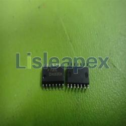
CD4016BCN
Compatible with a wide voltage range of 3V to 15V
品質保證
品質保證
從我們的供應鍊網路採購的所有零件都經過嚴格的進貨檢驗流程。 這種細緻的檢查可確保客戶收到的零件是正品並符合要求的標準。 此外,我們還保存這些檢查的詳細記錄,以確保整個供應鏈的透明度和可追溯性。


認證
我們已成功獲得各項認證標準,並建立了自己的專業檢測實驗室。 這確保了我們向客戶提供的每件產品都符合最高的品質標準。 我們遵守嚴格的測試協議,以保持我們產品的一致性和準確性。 為了確保我們的產品是原裝正品,我們還與信譽良好的第三方檢測機構合作進行嚴格的品質測試。 我們對品質的承諾延伸到滿足行業、法律、監管和 ISO 9001:2015 的要求。
運輸與付款
運輸與付款
關於運送
我們通常會在幾個工作日內通過可靠的運輸公司(例如 FedEx、SF、UPS 或 DHL)運送訂單。 我們還支持其他運輸方式。 如果您想詢問具體的運輸細節或費用,請隨時與我們聯繫。


關於付款
我們接受多種支付方式,包括VISA、MasterCard、銀聯、西聯、PayPal等渠道。
如果您有特定的付款方式或想詢問費率和其他詳細信息,請隨時與我們聯繫。

電匯

Paypal

信用卡

西聯匯款

速匯金
服務與包裝
服務與包裝
About After Sales Service
All Parts Extended Quality Guarantee
自發貨之日起 90 天內發起申請。
與我們的工作人員確認退貨或換貨。
保持貨物收到時的原始狀態。
最後請注意,退貨或換貨的資格取決於對退貨商品實際狀況的評估。 在完成退貨或換貨流程之前,我們將評估收到的貨物。 如果您對退貨或換貨有任何疑問或需要進一步幫助,請隨時通過以下方式聯絡我們: [email protected]
關於包裝
在包裝方面,我們的產品均精心包裝在防靜電袋中,以提供ESD防靜電保護。 外包裝堅固耐用且閉合牢固。 我們支持各種包裝方法,例如捲帶式、切帶式、管式或託盤式。

例子

捲帶式

剪膠帶

管或託盤
CD4016BCN 數據表
價格 (USD)
| 數量 | 單價 | 總價 |
|---|---|---|
| 1 | $0.309 | $0.31 |
| 200 | $0.119 | $23.80 |
| 500 | $0.115 | $57.50 |
| 1000 | $0.113 | $113.00 |
這些價格會受到市場波動的影響,需要提交報價才能取得最新價格。
詳細說明
In summary, the CD4016BCN is a reliable and efficient quad bilateral switch IC that is well-suited for a range of analog signal switching applications. Its high level of integration, low power consumption, and precise signal control capabilities make it a valuable component in electronic circuits where signal manipulation is critical. Whether used in audio systems, video equipment, or signal routing designs, the CD4016BCN provides the performance and reliability engineers need for their projects
主要特徵
- Wide supply voltage range: 3V to 15V
- Wide range of digital and analog switching: ±7.5 VPEAK
- “ON” Resistance for 15V operation: 400Ω (typ)
- Matched “ON” Resistance over 15V signal input:
- ∆RON = 10Ω (typ)
- High degree of linearity:
- 0.4% distortion (typ)
- @ fIS = 1 kHz, VIS = 5 Vp-p,
- VDD−VSS = 10V, RL = 10 kΩ
- Extremely low “OFF” switch leakage:
- 0.1 nA (typ.)
- @ VDD − VSS = 10V
- TA = 25°C
- Extremely high control input impedance: 1012Ω (typ)
- Low crosstalk between switches:
- −50 dB (typ.)
- @ fIS = 0.9 MHz, RL = 1 kΩ
- Frequency response, switch “ON”: 40 MHz (typ)
規格
以下是所選零件的基本參數,涉及零件的特性及其所屬類別。
| Pbfree Code | Yes | Rohs Code | Yes |
| Part Life Cycle Code | Active | Part Package Code | DIP |
| Pin Count ! | 14 | Reach Compliance Code | |
| Analog IC - Other Type | SPST | JESD-30 Code | R-PDIP-T14 |
| JESD-609 Code | e3 | Length | 19.18 mm |
| Moisture Sensitivity Level | NOT APPLICABLE | Number of Channels | 1 |
| Number of Functions | 4 | Number of Terminals | 14 |
| On-state Resistance Match-Nom | 15 Ω | On-state Resistance-Max (Ron) | 2000 Ω |
| Operating Temperature-Max | 85 °C | Operating Temperature-Min | -40 °C |
| Package Body Material | PLASTIC/EPOXY | Package Code | DIP |
| Package Shape | RECTANGULAR | Package Style | IN-LINE |
| Peak Reflow Temperature (Cel) | NOT APPLICABLE | Qualification Status ! | COMMERCIAL |
| Seated Height-Max | 5.08 mm | Supply Voltage-Max (Vsup) | 15 V |
| Supply Voltage-Min (Vsup) | 3 V | Supply Voltage-Nom (Vsup) | 10 V |
| Surface Mount ! | NO | Switch-off Time-Max | 25 ns |
| Switch-on Time-Max | 40 ns | Temperature Grade ! | INDUSTRIAL |
| Terminal Finish | MATTE TIN | Terminal Form ! | THROUGH-HOLE |
| Terminal Pitch ! | 2.54 mm | Terminal Position | DUAL |
| Time@Peak Reflow Temperature-Max (s) | NOT APPLICABLE | Width | 7.62 mm |
數據表 PDF
數據表記錄了器件的特性、絕對最大額定值、應用等,這對於作為器件特定應用的整體指南大有裨益。
常見問題解答
What is CD4016BCN?
The CD4016BCN is a quad bilateral switch IC (integrated circuit) designed by Texas Instruments. It is ideal for applications requiring analog signal switching and transmission, such as audio signal routing, signal multiplexing, and analog multiplexers.
How Does CD4016BCN Work?
The CD4016BCN works by providing four independent bilateral switches that control the flow of analog signals. Each switch can be turned on or off using control signals, allowing the user to select different input and output connections. This enables the IC to act as a versatile analog signal routing and switching component.
How Many Pins does CD4016BCN have and What are the Functions of the Pinout Configuration?
The CD4016BCN is housed in a 14-pin PDIP (Plastic Dual In-Line Package) package. The pinout configuration includes:
- VDD: Positive power supply pin.
- VSS: Ground pin.
- Control Inputs (1, 2, 3, 4): Control pins for each switch.
- Analog Switches (1, 2, 3, 4): Analog signal input and output pins for each switch.
What are the Pros and Cons of CD4016BCN?
Pros:
- Multiple Switches: Provides four independent switches in a single IC, enabling multiple signal routing options.
- Versatility: Suitable for a wide range of analog signal switching applications.
- Simple Control: Can be easily controlled using digital logic signals.
- Low Cost: Offers cost-effective analog signal switching solution.
Cons:
- Signal Range: Limited to handling low-frequency and moderate voltage signals.
- On-Resistance: Switches have finite on-resistance, which can affect signal integrity in some applications.
- Non-Rail-to-Rail Operation: May not be suitable for applications requiring full swing signal handling.
Are There Any Equivalents/Alternatives to CD4016BCN for Recommendation?
- The DG406 from Intersil is an equivalent quad bilateral switch IC.
- Alternatives to the CD4016BCN include the 74HC4066 from Nexperia and the MAX4066 from Maxim Integrated.
推薦零件
-
![CD4093BCMX]()
CD4093BCMX is a powerful and precise quad NAND Schmitt trigger for digital designs
製造商: Onsemi 包裝/箱: 14-SOIC(0.154",3.90mmWidth)
7,601 有存貨
貨物週期: 3~7 天
最小訂購量為 1
-
![CD40193BCN]()
The CD40193BCN is a Counter IC that can synchronize and count up to 4-bits of binary information
製造商: Onsemi 包裝/箱: 16-DIP(0.300",7.62mm)
7,680 有存貨
貨物週期: 3~7 天
最小訂購量為 1