恭喜您提交成功
 提交失敗
提交失敗

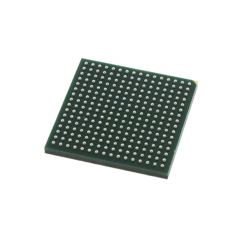
AM4378BZDND80
491-Pin NFBGA Tray
-
製造商零件號 # : AM4378BZDND80
-
包裝/封裝: NFBGA-491
-
製造商: Texas Instruments
-
產品分類 : Microprocessors
品質保證
品質保證
從我們的供應鍊網路採購的所有零件都經過嚴格的進貨檢驗流程。 這種細緻的檢查可確保客戶收到的零件是正品並符合要求的標準。 此外,我們還保存這些檢查的詳細記錄,以確保整個供應鏈的透明度和可追溯性。


認證
我們已成功獲得各項認證標準,並建立了自己的專業檢測實驗室。 這確保了我們向客戶提供的每件產品都符合最高的品質標準。 我們遵守嚴格的測試協議,以保持我們產品的一致性和準確性。 為了確保我們的產品是原裝正品,我們還與信譽良好的第三方檢測機構合作進行嚴格的品質測試。 我們對品質的承諾延伸到滿足行業、法律、監管和 ISO 9001:2015 的要求。
運輸與付款
運輸與付款
關於運送
我們通常會在幾個工作日內通過可靠的運輸公司(例如 FedEx、SF、UPS 或 DHL)運送訂單。 我們還支持其他運輸方式。 如果您想詢問具體的運輸細節或費用,請隨時與我們聯繫。


關於付款
我們接受多種支付方式,包括VISA、MasterCard、銀聯、西聯、PayPal等渠道。
如果您有特定的付款方式或想詢問費率和其他詳細信息,請隨時與我們聯繫。

電匯

Paypal

信用卡

西聯匯款

速匯金
服務與包裝
服務與包裝
About After Sales Service
All Parts Extended Quality Guarantee
自發貨之日起 90 天內發起申請。
與我們的工作人員確認退貨或換貨。
保持貨物收到時的原始狀態。
最後請注意,退貨或換貨的資格取決於對退貨商品實際狀況的評估。 在完成退貨或換貨流程之前,我們將評估收到的貨物。 如果您對退貨或換貨有任何疑問或需要進一步幫助,請隨時通過以下方式聯絡我們: [email protected]
關於包裝
在包裝方面,我們的產品均精心包裝在防靜電袋中,以提供ESD防靜電保護。 外包裝堅固耐用且閉合牢固。 我們支持各種包裝方法,例如捲帶式、切帶式、管式或託盤式。

例子

捲帶式

剪膠帶

管或託盤
AM4378BZDND80 數據表

目前的價格方案正在編制中。請聯絡我們的客戶服務團隊獲取最新的價格資訊。感謝您的理解和支援!
詳細說明
The TI AM437x high-performance processors are equipped with advanced features, making them ideal for applications requiring rich graphical user interfaces and real-time processing capabilities. The inclusion of a coprocessor for industrial communication protocols sets these processors apart, allowing for seamless integration into a wide range of industrial systems. In addition, the support for high-level operating systems, such as Linux, ensures compatibility with a variety of software environments. The upgraded peripherals, including memory options like QSPI-NOR and LPDDR2, further enhance the performance of these processors, making them a versatile solution for diverse applications
主要特徵
- Highlights
- Sitara™ ARM® Cortex®-A9 32-Bit RISC Processor With Processing Speed up to 1000 MHz
- NEON™ SIMD Coprocessor and Vector Floating Point (VFPv3) Coprocessor
- 32KB of Both L1 Instruction and Data Cache
- 256KB of L2 Cache or L3 RAM
- 32-Bit LPDDR2, DDR3, and DDR3L Support
- General-Purpose Memory Support (NAND, NOR, SRAM) Supporting up to 16-Bit ECC
- SGX530 Graphics Engine
- Display Subsystem
- Programmable Real-Time Unit Subsystem and Industrial Communication Subsystem (PRU-ICSS)
- Real-Time Clock (RTC)
- Up to Two USB 2.0 High-Speed Dual-Role (Host or Device) Ports With Integrated PHY
- 10, 100, and 1000 Ethernet Switch Supporting up to Two Ports
- Serial Interfaces:
- Two Controller Area Network (CAN) Ports
- Six UARTs, Two McASPs, Five McSPIs, Three I2C Ports, One QSPI, and One HDQ or 1-Wire
- Security
- Crypto Hardware Accelerators (AES, SHA, RNG, DES, and 3DES)
- Secure Boot (Avaliable Only on AM437x High-Security [AM437xHS] Devices)
- Two 12-Bit Successive Approximation Register (SAR) ADCs
- Up to Three 32-Bit Enhanced Capture (eCAP) Modules
- Up to Three Enhanced Quadrature Encoder Pulse (eQEP) Modules
- Up to Six Enhanced High-Resolution PWM (eHRPWM) Modules
- Sitara™ ARM® Cortex®-A9 32-Bit RISC Processor With Processing Speed up to 1000 MHz
- MPU Subsystem
- ARM Cortex-A9 32-Bit RISC Microprocessor With Processing Speed up to 1000 MHz
- 32KB of Both L1 Instruction and Data Cache
- 256KB of L2 Cache (Option to Configure as L3 RAM)
- 256KB of On-Chip Boot ROM
- 64KB of On-Chip RAM
- Secure Control Module (SCM) (Avaliable Only on AM437xHS Devices)
- Emulation and Debug
- JTAG
- Embedded Trace Buffer
- Interrupt Controller
- On-Chip Memory (Shared L3 RAM)
- 256KB of General-Purpose On-Chip Memory Controller (OCMC) RAM
- Accessible to All Masters
- Supports Retention for Fast Wakeup
- Up to 512KB of Total Internal RAM
(256KB of ARM Memory Configured as L3 RAM + 256KB of OCMC RAM)
- External Memory Interfaces (EMIFs)
- DDR Controllers:
- LPDDR2: 266-MHz Clock (LPDDR2-533 Data Rate)
- DDR3 and DDR3L: 400-MHz Clock (DDR-800 Data Rate)
- 32-Bit Data Bus
- 2GB of Total Addressable Space
- Supports One x32, Two x16, or Four x8 Memory Device Configurations
- DDR Controllers:
- General-Purpose Memory Controller (GPMC)
- Flexible 8- and 16-Bit Asynchronous Memory Interface With up to Seven Chip Selects (NAND, NOR, Muxed-NOR, and SRAM)
- Uses BCH Code to Support 4-, 8-, or 16-Bit ECC
- Uses Hamming Code to Support 1-Bit ECC
- Error Locator Module (ELM)
- Used With the GPMC to Locate Addresses of Data Errors From Syndrome Polynomials Generated Using a BCH Algorithm
- Supports 4-, 8-, and 16-Bit Per 512-Byte Block Error Location Based on BCH Algorithms
- Programmable Real-Time Unit Subsystem and Industrial Communication Subsystem (PRU-ICSS)
- Supports Protocols such as EtherCAT®, PROFIBUS®, PROFINET®, and EtherNet/IP™, EnDat 2.2, and More
- Two Programmable Real-Time Units (PRUs) Subsystems With Two PRU Cores Each
- Each Core is a 32-Bit Load and Store RISC Processor Capable of Running at 200 MHz
- 12KB (PRU-ICSS1), 4KB (PRU-ICSS0) of Instruction RAM With Single-Error Detection (Parity)
- 8KB (PRU-ICSS1), 4KB (PRU-ICSS0) of Data RAM With Single-Error Detection (Parity)
- Single-Cycle 32-Bit Multiplier With 64-Bit Accumulator
- Enhanced GPIO Module Provides Shift-In and Shift-Out Support and Parallel Latch on External Signal
- 12KB (PRU-ICSS1 Only) of Shared RAM With Single-Error Detection (Parity)
- Three 120-Byte Register Banks Accessible by Each PRU
- Interrupt Controller Module (INTC) for Handling System Input Events
- Local Interconnect Bus for Connecting Internal and External Masters to the Resources Inside the PRU-ICSS
- Peripherals Inside the PRU-ICSS
- One UART Port With Flow Control Pins, Supports up to 12 Mbps
- One eCAP Module
- Two MII Ethernet Ports that Support Industrial Ethernet, such as EtherCAT
- One MDIO Port
- Industrial Communication is Supported by Two PRU-ICSS Subsystems
- Power, Reset, and Clock Management (PRCM) Module
- Controls the Entry and Exit of Deep-Sleep Modes
- Responsible for Sleep Sequencing, Power Domain Switch-Off Sequencing, Wake-Up Sequencing, and Power Domain Switch-On Sequencing
- Clocks
- Integrated High-Frequency Oscillator Used to Generate a Reference Clock (19.2, 24, 25, and 26 MHz) for Various System and Peripheral Clocks
- Supports Individual Clock Enable and Disable Control for Subsystems and Peripherals to Facilitate Reduced Power Consumption
- Five ADPLLs to Generate System Clocks (MPU Subsystem, DDR Interface, USB, and Peripherals [MMC and SD, UART, SPI, I2C], L3, L4, Ethernet, GFX [SGX530], and LCD Pixel Clock)
- Power
- Two Nonswitchable Power Domains (RTC and Wake-Up Logic [WAKE-UP])
- Three Switchable Power Domains (MPU Subsystem, SGX530 [GFX], Peripherals and Infrastructure [PER])
- Dynamic Voltage Frequency Scaling (DVFS)
- Real-Time Clock (RTC)
- Real-Time Date (Day, Month, Year, and Day of Week) and Time (Hours, Minutes, and Seconds) Information
- Internal 32.768-kHz Oscillator, RTC Logic, and 1.1-V Internal LDO
- Independent Power-On-Reset (RTC_PWRONRSTn) Input
- Dedicated Input Pin (RTC_WAKEUP) for External Wake Events
- Programmable Alarm Can Generate Internal Interrupts to the PRCM for Wakeup or Cortex-A9 for Event Notification
- Programmable Alarm Can Be Used With External Output (RTC_PMIC_EN) to Enable the Power-Management IC to Restore Non-RTC Power Domains
- Peripherals
- Up to Two USB 2.0 High-Speed Dual-Role (Host or Device) Ports With Integrated PHY
- Up to Two Industrial Gigabit Ethernet MACs
(10, 100, and 1000 Mbps)- Integrated Switch
- Each MAC Supports MII, RMII, and RGMII and MDIO Interfaces
- Ethernet MACs and Switch Can Operate Independent of Other Functions
- IEEE 1588v2 Precision Time Protocol (PTP)
- Up to Two CAN Ports
- Supports CAN Version 2 Parts A and B
- Up to Two Multichannel Audio Serial Ports (McASPs)
- Transmit and Receive Clocks up to 50 MHz
- Up to Four Serial Data Pins Per McASP Port With Independent TX and RX Clocks
- Supports Time Division Multiplexing (TDM), Inter-IC Sound (I2S), and Similar Formats
- Supports Digital Audio Interface Transmission (SPDIF, IEC60958-1, and AES-3 Formats)
- FIFO Buffers for Transmit and Receive (256 Bytes)
- Up to Six UARTs
- All UARTs Support IrDA and CIR Modes
- All UARTs Support RTS and CTS Flow Control
- UART1 Supports Full Modem Control
- Up to Five Master and Slave McSPIs
- McSPI0–McSPI2 Support up to Four Chip Selects
- McSPI3 and McSPI4 Support up to Two Chip Selects
- Up to 48 MHz
- One Quad-SPI
- Supports eXecute In Place (XIP) from Serial NOR FLASH
- One Dallas 1-Wire® and HDQ Serial Interface
- Up to Three MMC, SD, and SDIO Ports
- 1-, 4-, and 8-Bit MMC, SD, and SDIO Modes
- 1.8- or 3.3-V Operation on All Ports
- Up to 48-MHz Clock
- Supports Card Detect and Write Protect
- Complies With MMC4.3 and SD and SDIO 2.0 Specifications
- Up to Three I2C Master and Slave Interfaces
- Standard Mode (up to 100 kHz)
- Fast Mode (up to 400 kHz)
- Up to Six Banks of General-Purpose I/O (GPIO)
- 32 GPIOs per Bank (Multiplexed With Other Functional Pins)
- GPIOs Can be Used as Interrupt Inputs (up to Two Interrupt Inputs per Bank)
- Up to Three External DMA Event Inputs That Can Also be Used as Interrupt Inputs
- Twelve 32-Bit General-Purpose Timers
- DMTIMER1 is a 1-ms Timer Used for Operating System (OS) Ticks
- DMTIMER4–DMTIMER7 are Pinned Out
- One Public Watchdog Timer
- One Free-Running, High-Resolution 32-kHz Counter (synctimer32K)
- One Secure Watchdog Timer (Avaliable Only on AM437xHS Devices)
- SGX530 3D Graphics Engine
- Tile-Based Architecture Delivering up to 20M Poly/sec
- Universal Scalable Shader Engine is a Multithreaded Engine Incorporating Pixel and Vertex Shader Functionality
- Advanced Shader Feature Set in Excess of Microsoft VS3.0, PS3.0, and OGL2.0
- Industry Standard API Support of Direct3D Mobile, OGL-ES 1.1 and 2.0
- Fine-Grained Task Switching, Load Balancing, and Power Management
- Advanced Geometry DMA-Driven Operation for Minimum CPU Interaction
- Programmable High-Quality Image Anti-Aliasing
- Fully Virtualized Memory Addressing for OS Operation in a Unified Memory Architecture
- Display Subsystem
- Display Modes
- Programmable Pixel Memory Formats (Palletized: 1-, 2-, 4-, and 8-Bits Per Pixel; RGB 16- and 24-Bits Per Pixel; and YUV 4:2:2)
- 256- × 24-Bit Entries Palette in RGB
- Up to 2048 × 2048 Resolution
- Display Support
- Four Types of Displays Are Supported: Passive and Active Colors; Passive and Active Monochromes
- 4- and 8-Bit Monochrome Passive Panel Interface Support (15 Grayscale Levels Supported Using Dithering Block)
- RGB 8-Bit Color Passive Panel Interface Support (3,375 Colors Supported for Color Panel Using Dithering Block)
- RGB 12-, 16-, 18-, and 24-Bit Active Panel Interface Support (Replicated or Dithered Encoded Pixel Values)
- Remote Frame Buffer (Embedded in the LCD Panel) Support Through the RFBI Module
- Partial Refresh of the Remote Frame Buffer Through the RFBI Module
- Partial Display
- Multiple Cycles Output Format on 8-, 9-, 12-, and 16-Bit Interface (TDM)
- Signal Processing
- Overlay and Windowing Support for One Graphics Layer (RGB or CLUT) and Two Video Layers (YUV 4:2:2, RGB16, and RGB24)
- RGB 24-Bit Support on the Display Interface, Optionally Dithered to RGB 18‑Bit Pixel Output Plus 6-Bit Frame Rate Control (Spatial and Temporal)
- Transparency Color Key (Source and Destination)
- Synchronized Buffer Update
- Gamma Curve Support
- Multiple-Buffer Support
- Cropping Support
- Color Phase Rotation
- Display Modes
- Two 12-Bit SAR ADCs (ADC0, ADC1)
- 867K Samples Per Second
- Input Can Be Selected from Any of the Eight Analog Inputs Multiplexed Through an 8:1 Analog Switch
- ADC0 Can Be Configured to Operate as a 4‑, 5-, or 8-Wire Resistive Touch Screen Controller (TSC)
- Up to Three 32-Bit eCAP Modules
- Configurable as Three Capture Inputs or Three Auxiliary PWM Outputs
- Up to Six Enhanced eHRPWM Modules
- Dedicated 16-Bit Time-Base Counter With Time and Frequency Controls
- Configurable as Six Single-Ended, Six Dual-Edge Symmetric, or Three Dual-Edge Asymmetric Outputs
- Up to Three 32-Bit eQEP Modules
- Device Identification
- Factory Programmable Electrical Fuse Farm (FuseFarm)
- Production ID
- Device Part Number (Unique JTAG ID)
- Device Revision (Readable by Host ARM)
- Security Keys (Avaliable Only on AM437xHS Devices)
- Feature Identification
- Factory Programmable Electrical Fuse Farm (FuseFarm)
- Debug Interface Support
- JTAG and cJTAG for ARM (Cortex-A9 and PRCM) and PRU-ICSS Debug
- Supports Real-Time Trace Pins (for Cortex-A9)
- 64-KB Embedded Trace Buffer (ETB)
- Supports Device Boundary Scan
- Supports IEEE 1500
- DMA
- On-Chip Enhanced DMA Controller (EDMA) Has Three Third-Party Transfer Controllers (TPTCs) and One Third-Party Channel Controller (TPCC), Which Supports up to 64 Programmable Logical Channels and Eight QDMA Channels
- EDMA is Used for:
- Transfers to and from On-Chip Memories
- Transfers to and from External Storage (EMIF, GPMC, and Slave Peripherals)
- InterProcessor Communication (IPC)
- Integrates Hardware-Based Mailbox for IPC and Spinlock for Process Synchronization Between the Cortex-A9, PRCM, and PRU-ICSS
- Boot Modes
- Boot Mode is Selected Through Boot Configuration Pins Latched on the Rising Edge of the PWRONRSTn Reset Input Pin
- Camera
- Dual Port 8- and 10-Bit BT656 Interface
- Dual Port 8- and 10-Bit Including External Syncs
- Single Port 12-Bit
- YUV422/RGB422 and BT656 Input Format
- RAW Format
- Pixel Clock Rate up to 75 MHz
- Package
- 491-Pin BGA Package (17-mm × 17-mm) (ZDN Suffix), 0.65-mm Ball Pitch With Via Channel Array Technology to Enable Low-Cost Routing
規格
以下是所選零件的基本參數,涉及零件的特性及其所屬類別。
| Arm CPU | 1 Arm Cortex-A9 | Arm (max) (MHz) | 800, 1000 |
| Coprocessors | GPU, PRU-ICSS | CPU | 32-bit |
| Graphics acceleration | 1 3D | Display type | 1 LCD |
| Protocols | EtherNet/IP, Ethernet, Profibus, Profinet, Sercos | Ethernet MAC | 2-Port 1Gb switch |
| Hardware accelerators | PRU-ICSS, SGX530 Graphics, Security Accelerator | Features | General purpose, Networking |
| Operating system | Linux, RTOS | Security | Cryptography, Debug security, Secure boot, Trusted execution environment |
| Rating | Catalog | Power supply solution | TPS65216, TPS65218D0 |
| Operating temperature range (°C) | -40 to 105, -40 to 90, 0 to 90 |
推薦零件
-
![AT91SAM7S512-MU]()
7,717 有存貨
貨物週期: 3~7 天
最小訂購量為 1
-
![AT91SAM7S256C-AU]()
5,866 有存貨
貨物週期: 3~7 天
最小訂購量為 1
-
![AT91SAM7S512-AU]()
7,749 有存貨
貨物週期: 3~7 天
最小訂購量為 1
-
![S9KEAZN64AMLC]()
32-bit ARM Cortex M0+ microcontroller with 64KB Flash memory, suitable for automotive applications
製造商: Nxp Semiconductors 包裝/箱: LQFP-32
7,408 有存貨
貨物週期: 3~7 天
最小訂購量為 1
-
![SPC5744PFK1AMLQ9]()
This NXP MCU is designed for high performance with a 32-bit architecture and a powerful 200MHz processor
製造商: Freescale Semiconductor 包裝/箱: LQFP-144
6,725 有存貨
貨物週期: 3~7 天
最小訂購量為 1
-
![AT91SAM9260B-CU]()
AT91SAM9260B-CU
$8.302 MPU RISC 16bit/32bit 180MHz 217-Pin LFBGA Tray
製造商: Microchip Technology 包裝/箱: LFBGA-217
8,501 有存貨
貨物週期: 3~7 天
最小訂購量為 1
-
![ATSAMC21J18A-AUT]()
MCU 32-bit ARM Cortex M0+ RISC 256KB Flash 5V 64-Pin TQFP T/R
製造商: Microchip Technology 包裝/箱: TQFP-64
9,175 有存貨
貨物週期: 3~7 天
最小訂購量為 1
-
![ATSAM3X4EA-CU]()
ATSAM3X4EA-CU
$4.597 The ATSAM3X4EA-CU is built on a CMOS technology platform, ensuring efficient and reliable performance
製造商: Microchip Technology 包裝/箱: LFBGA
5,297 有存貨
貨物週期: 3~7 天
最小訂購量為 1
-
![AMA3B1KK-KBR-B0]()
9,606 有存貨
貨物週期: 3~7 天
最小訂購量為 1
-
![S9S12G64AMLF]()
6,900 有存貨
貨物週期: 3~7 天
最小訂購量為 1
-
![UPD78F0502AMC-CAB-AX]()
UPD78F0502AMC-CAB-AX
$1.185 LSSOP-30-6.1mm Microcontroller Units (MCUs/MPUs/SOCs) ROHS
製造商: Renesas Electronics America Inc 包裝/箱: SOP-30
8,263 有存貨
貨物週期: 3~7 天
最小訂購量為 1
-
![LAMXO3LF-2100E-5BG256E]()
6,987 有存貨
貨物週期: 3~7 天
最小訂購量為 1
-
![S9S12ZVL32AMLCR]()
5,282 有存貨
貨物週期: 3~7 天
最小訂購量為 1
-
![SAM9X72T-I/4PB]()
Microprocessors - MPU ARM926 MPU,LVDS,CAN-FD,BGA,I TEMP,T&R
製造商: Microchip Technology 包裝/箱: BGA-240
6,113 有存貨
貨物週期: 3~7 天
最小訂購量為 1
-
![ATSAM4CMS8CC-AUT]()
ATSAM4CMS8CC-AUT
$8.602 This product belongs to the ARM-MSeries and comes in a 57 TQFP-100 package size (14x14)
製造商: Microchip Technology 包裝/箱: 100-TQFP
5,864 有存貨
貨物週期: 3~7 天
最小訂購量為 1
-
![ATSAM4CMP8CC-AUTR]()
ARM Microcontrollers - MCU TQFP, Green, IND, Crypto, MRLC, 512k, R
製造商: Microchip Technology 包裝/箱: 100-TQFP
9,949 有存貨
貨物週期: 3~7 天
最小訂購量為 1