恭喜您提交成功
 提交失敗
提交失敗

AD7002
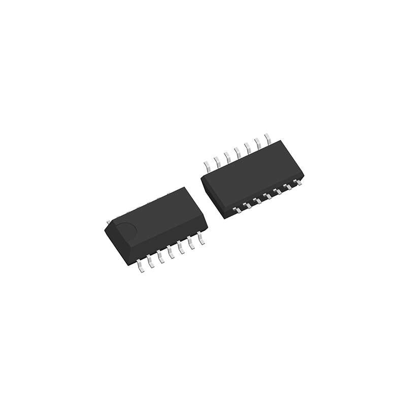
IC,DATA ACQ CODEC,1-CHANNEL,BICMOS,QFP,44PIN,PLASTIC
-
製造商零件號 # : AD7002
-
包裝/封裝: QFP
-
製造商: Analog Devices
-
產品分類 : Specialized ICs
品質保證
品質保證
從我們的供應鍊網路採購的所有零件都經過嚴格的進貨檢驗流程。 這種細緻的檢查可確保客戶收到的零件是正品並符合要求的標準。 此外,我們還保存這些檢查的詳細記錄,以確保整個供應鏈的透明度和可追溯性。


認證
我們已成功獲得各項認證標準,並建立了自己的專業檢測實驗室。 這確保了我們向客戶提供的每件產品都符合最高的品質標準。 我們遵守嚴格的測試協議,以保持我們產品的一致性和準確性。 為了確保我們的產品是原裝正品,我們還與信譽良好的第三方檢測機構合作進行嚴格的品質測試。 我們對品質的承諾延伸到滿足行業、法律、監管和 ISO 9001:2015 的要求。
運輸與付款
運輸與付款
關於運送
我們通常會在幾個工作日內通過可靠的運輸公司(例如 FedEx、SF、UPS 或 DHL)運送訂單。 我們還支持其他運輸方式。 如果您想詢問具體的運輸細節或費用,請隨時與我們聯繫。


關於付款
我們接受多種支付方式,包括VISA、MasterCard、銀聯、西聯、PayPal等渠道。
如果您有特定的付款方式或想詢問費率和其他詳細信息,請隨時與我們聯繫。

電匯

Paypal

信用卡

西聯匯款

速匯金
服務與包裝
服務與包裝
About After Sales Service
All Parts Extended Quality Guarantee
自發貨之日起 90 天內發起申請。
與我們的工作人員確認退貨或換貨。
保持貨物收到時的原始狀態。
最後請注意,退貨或換貨的資格取決於對退貨商品實際狀況的評估。 在完成退貨或換貨流程之前,我們將評估收到的貨物。 如果您對退貨或換貨有任何疑問或需要進一步幫助,請隨時通過以下方式聯絡我們: [email protected]
關於包裝
在包裝方面,我們的產品均精心包裝在防靜電袋中,以提供ESD防靜電保護。 外包裝堅固耐用且閉合牢固。 我們支持各種包裝方法,例如捲帶式、切帶式、管式或託盤式。

例子

捲帶式

剪膠帶

管或託盤
AD7002 數據表

目前的價格方案正在編制中。請聯絡我們的客戶服務團隊獲取最新的價格資訊。感謝您的理解和支援!
詳細說明
GENERAL DESCRIPTIONThe AD7002 is a complete low power, two-channel, input/output port with signal conditioning. The device is used as a baseband digitization subsystem, performing signal conversion between the DSP and the IF/RF sections in the Pan-European telephone system (GSM).FEATURES Single +5 V Supply Transmit Channel On-Chip GMSK Modulator Two 10-Bit D/A Converters Analog Reconstruction Filters Power-Down Mode Receive Channel Two Sigma-Delta A/D Converters FIR Digital Filters On-Chip Offset Calibration Power-Down Mode 3 Auxiliary D/A Converters Power-Down Modes On-Chip Voltage Reference Low Power 44-Lead PQFPAPPLICATIONS GSM PCN
主要特徵
- Single +5 V Supply
- Transmit Channel
- On-Chip GMSK Modulator
- Two 10-Bit D/A Converters
- Analog Reconstruction Filters
- Power-Down Mode
- Receive Channel
- Two Sigma-Delta A/D Converters
- FIR Digital Filters
- On-Chip Offset Calibration
- Power-Down Mode
- 3 Auxiliary D/A Converters
- Power-Down Modes
- On-Chip Voltage Reference
- Low Power
- 44-Lead PQFP
規格
以下是所選零件的基本參數,涉及零件的特性及其所屬類別。
| Rohs Code | No | Part Life Cycle Code | Obsolete |
| Reach Compliance Code | Input Type | SINGLE-ENDED | |
| JESD-30 Code | S-PQFP-G44 | JESD-609 Code | e0 |
| Number of Channels | 1 | Number of Terminals | 44 |
| Operating Temperature-Max | 85 °C | Operating Temperature-Min | -40 °C |
| Output | VOLTAGE | Package Body Material | PLASTIC/EPOXY |
| Package Code | QFP | Package Equivalence Code | QFP44,.57SQ,32 |
| Package Shape | SQUARE | Package Style | FLATPACK |
| Power Supplies ! | 5 V | Qualification Status ! | Not Qualified |
| Resolution | 10 um | Supply Current-Max | 30 mA |
| Supply Voltage-Nom | 5 V | Surface Mount ! | YES |
| Technology | BICMOS | Temperature Grade ! | INDUSTRIAL |
| Terminal Finish | Tin/Lead (Sn/Pb) | Terminal Form ! | GULL WING |
| Terminal Pitch ! | 0.8 mm | Terminal Position | QUAD |
數據表 PDF
數據表記錄了器件的特性、絕對最大額定值、應用等,這對於作為器件特定應用的整體指南大有裨益。
常見問題解答
What is AD7002?
The AD7002 is a dual, 12-bit, low power, successive approximation analog-to-digital converter (ADC) designed by Analog Devices. It is suitable for applications requiring moderate resolution and low power consumption, such as industrial control systems, data acquisition, and instrumentation.
How Does AD7002 Work?
The AD7002 operates by converting analog input signals into digital data through a successive approximation process. It features dual ADC channels for simultaneous conversion and a low-power design for energy-efficient operation. The converter offers 12-bit resolution and a flexible interface for integrating into various system designs.
How Many Pins does AD7002 have and What are the Functions of the Pinout Configuration?
The AD7002 is housed in a 16-lead SSOP (Shrink Small Outline Package) package. The pinout configuration includes:
- VDD, GND: Power supply and ground pins, respectively.
- AIN0, AIN1: Analog input channels for the dual ADC.
- REF, CAP, OV: Reference voltage, external capacitor, and overvoltage pins.
- DOUTA, DOUTB: Digital output pins for each ADC channel.
- CLK, CS, SCLK: Clock and control interface pins.
What are the Pros and Cons of AD7002?
Pros:
- Dual ADC Channels: Allows for simultaneous conversion of two analog signals.
- Low Power Consumption: Ideal for applications where power efficiency is critical.
- 12-bit Resolution: Provides moderate resolution for accurate digital conversion.
- Flexible Interface: Supports a versatile interface for easy integration into systems.
- Compact Package: The 16-lead SSOP package offers a space-efficient design.
Cons:
- Moderate Resolution: May not be suitable for applications requiring higher resolution.
- Speed Limitations: Limited maximum sampling rate compared to high-speed ADCs.
- External Components: Some applications may require additional external components for performance optimization.
Are There Any Equivalents/Alternatives to AD7002 for Recommendation?
- The ADS7822 from Texas Instruments is a comparable dual 12-bit ADC.
- Alternative options to the AD7002 include the MAX1216 from Maxim Integrated and the LTC1867 from Analog Devices.
推薦零件
-
![AD9516-3]()
5,144 有存貨
貨物週期: 3~7 天
最小訂購量為 1
-
![ADXL190WQC]()
IC SPECIALTY ANALOG CIRCUIT, CDSO14, HERMETIC SEALED, CERPACK-14, Analog IC:Other
製造商: Analog Devices 包裝/箱: SOP-14
5,744 有存貨
貨物週期: 3~7 天
最小訂購量為 1