恭喜您提交成功
 提交失敗
提交失敗
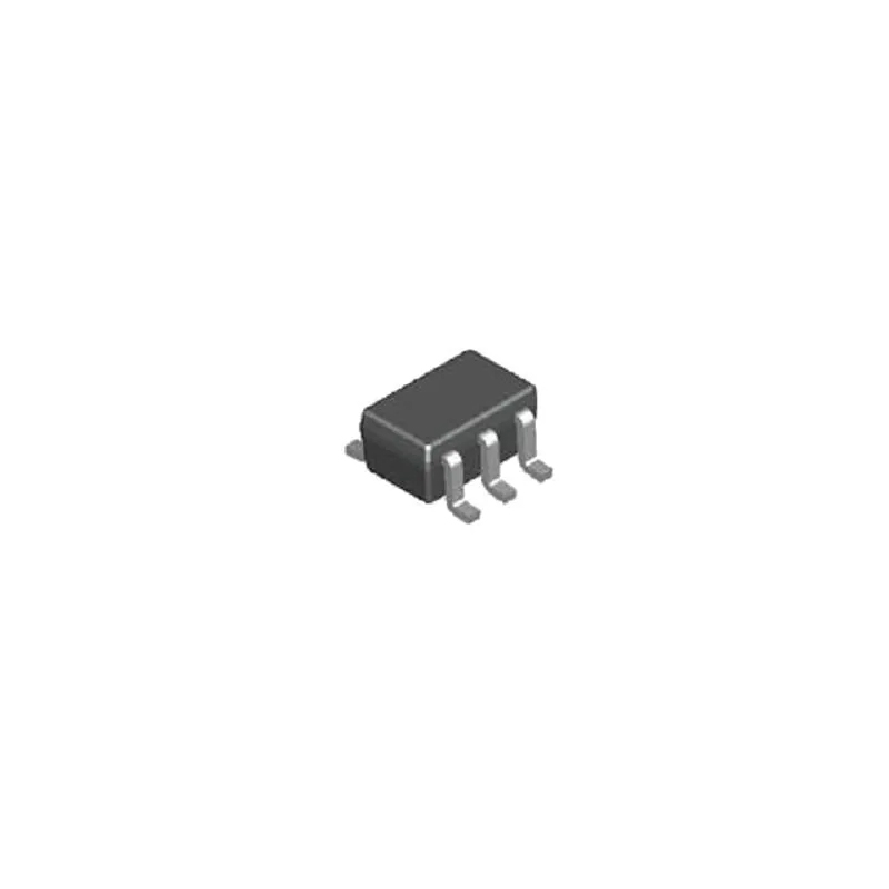
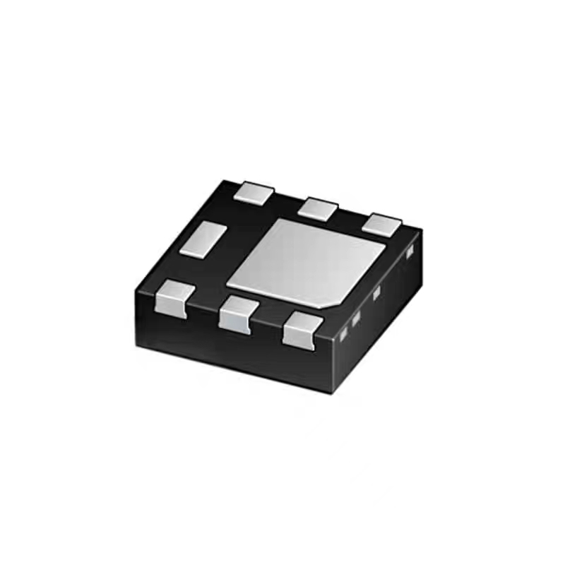
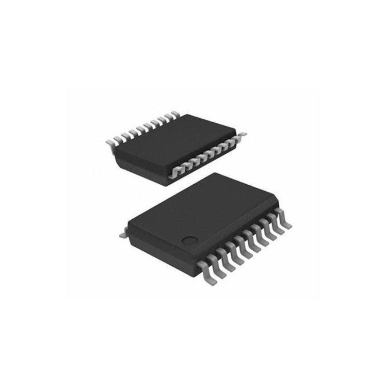
74LVC2G34GW,125
Buffers & Line Drivers 74LVC2G34GW/SOT363/SC-88
74LVC2G34GW,125
Buffers & Line Drivers 74LVC2G34GW/SOT363/SC-88
品質保證
品質保證
從我們的供應鍊網路採購的所有零件都經過嚴格的進貨檢驗流程。 這種細緻的檢查可確保客戶收到的零件是正品並符合要求的標準。 此外,我們還保存這些檢查的詳細記錄,以確保整個供應鏈的透明度和可追溯性。


認證
我們已成功獲得各項認證標準,並建立了自己的專業檢測實驗室。 這確保了我們向客戶提供的每件產品都符合最高的品質標準。 我們遵守嚴格的測試協議,以保持我們產品的一致性和準確性。 為了確保我們的產品是原裝正品,我們還與信譽良好的第三方檢測機構合作進行嚴格的品質測試。 我們對品質的承諾延伸到滿足行業、法律、監管和 ISO 9001:2015 的要求。
運輸與付款
運輸與付款
關於運送
我們通常會在幾個工作日內通過可靠的運輸公司(例如 FedEx、SF、UPS 或 DHL)運送訂單。 我們還支持其他運輸方式。 如果您想詢問具體的運輸細節或費用,請隨時與我們聯繫。


關於付款
我們接受多種支付方式,包括VISA、MasterCard、銀聯、西聯、PayPal等渠道。
如果您有特定的付款方式或想詢問費率和其他詳細信息,請隨時與我們聯繫。

電匯

Paypal

信用卡

西聯匯款

速匯金
服務與包裝
服務與包裝
About After Sales Service
All Parts Extended Quality Guarantee
自發貨之日起 90 天內發起申請。
與我們的工作人員確認退貨或換貨。
保持貨物收到時的原始狀態。
最後請注意,退貨或換貨的資格取決於對退貨商品實際狀況的評估。 在完成退貨或換貨流程之前,我們將評估收到的貨物。 如果您對退貨或換貨有任何疑問或需要進一步幫助,請隨時通過以下方式聯絡我們: [email protected]
關於包裝
在包裝方面,我們的產品均精心包裝在防靜電袋中,以提供ESD防靜電保護。 外包裝堅固耐用且閉合牢固。 我們支持各種包裝方法,例如捲帶式、切帶式、管式或託盤式。

例子

捲帶式

剪膠帶

管或託盤
74LVC2G34GW,125 數據表
價格 (USD)
| 數量 | 單價 | 總價 |
|---|---|---|
| 5 | $0.061 | $0.30 |
| 50 | $0.059 | $2.95 |
| 150 | $0.059 | $8.85 |
| 500 | $0.058 | $29.00 |
這些價格會受到市場波動的影響,需要提交報價才能取得最新價格。
詳細說明
The 74LVC2G34GW,125 is a dual inverter buffer IC. It contains two independent inverter buffer circuits, each capable of inverting the input signal.
主要特徵
- Dual Inverter Buffers: The IC features two independent inverter buffer circuits, each capable of inverting the input signal.
- High-Speed Operation: The IC is designed for high-speed digital signal processing.
- Wide Operating Voltage Range: It can operate over a wide range of supply voltages, making it compatible with various digital logic families.
- Low Voltage Operation: The "LVC" in its name indicates low voltage operation, designed to work at lower supply voltage levels.
- Low Power Consumption: The IC is designed for low power consumption, making it suitable for energy-efficient applications.
- Compact Package: This IC is often available in compact surface-mount packages for easy integration into electronic circuits.
應用
The 74LVC2G34GW,125 dual inverter buffer IC is used in various digital logic and signal inversion applications, including but not limited to:
- Signal inversion in digital systems.
- General-purpose digital logic operations.
- Signal buffering and amplification.
- Digital signal processing and waveform shaping.

規格
以下是所選零件的基本參數,涉及零件的特性及其所屬類別。
| Product Name | 74LVC2G34GW,125 | Product Type ! | Dual Buffer |
| Manufacturer | Nexperia | Number of Buffers | 2 |
| Supply Voltage | 1.65V to 5.5V | Operating Temperature Range ! | -40°C to +125°C |
| Package / Case | SC-88A (SOT353) | Product Category ! | Buffers & Line Drivers |
| RoHS | Details | Number of Input Lines | 2 Input |
| Number of Output Lines | 2 Output | Polarity | Non-Inverting |
| High Level Output Current ! | - 32 mA | Low Level Output Current ! | 32 mA |
| Quiescent Current ! | 100 nA | Supply Voltage - Max | 5.5 V |
| Supply Voltage - Min | 1.65 V | Operating Supply Current | 4 uA |
| Minimum Operating Temperature | - 40 C | Maximum Operating Temperature ! | + 125 C |
| Mounting Style | SMD/SMT | Brand | Nexperia |
| Function | Buffer | Height | 1 mm |
| Input Signal Type | Single-Ended | Length | 2.2 mm |
| Logic Family | LVC | Number of Channels | 2 |
| Operating Supply Voltage ! | 1.8 V, 2.5 V, 3.3 V, 5 V | Pd - Power Dissipation | 250 mW |
| Propagation Delay Time | 2.5 ns at 2.7 V, 2.2 ns at 3.3 V, 1.9 ns at 5 V | Factory Pack Quantity | 3000 |
| Subcategory | Logic ICs | Supply Current - Max | 40 uA |
| Technology | CMOS | Width | 1.35 mm |
| Part # Aliases | 935273783125 | Unit Weight | 0.035274 oz |
| Series | 74LVC | Product Status | Active |
| Logic Type | Buffer, Non-Inverting | Number of Elements | 2 |
| Number of Bits per Element | 1 | Output Type | Push-Pull |
| Current - Output High, Low | 32mA, 32mA | Voltage - Supply | 1.65V ~ 5.5V |
| Operating Temperature ! | -40°C ~ 125°C (TA) | Mounting Type | Surface Mount |
| Supplier Device Package | 6-TSSOP | Base Product Number | 74LVC2G34 |
數據表 PDF
數據表記錄了器件的特性、絕對最大額定值、應用等,這對於作為器件特定應用的整體指南大有裨益。
常見問題解答
What is 74LVC2G34GW?
The 74LVC2G34GW is a dual buffer/line driver designed by Nexperia. It is ideal for applications requiring voltage level translation and signal amplification, such as data communication, interface logic level conversion, and general-purpose buffering.
How Does 74LVC2G34GW Work?
The 74LVC2G34GW works by taking input signals at one voltage level and translating them to a different voltage level while providing signal buffering and driving capabilities. It can handle both uni-directional and bi-directional voltage level translations, making it suitable for a wide range of applications.
How Many Pins does 74LVC2G34GW have and What are the Functions of the Pinout Configuration?
The 74LVC2G34GW is housed in a 8-pin TSSOP (Thin Shrink Small Outline Package) package. The pinout configuration includes:
- A: Input A for buffer 1 and buffer 2.
- Y: Output Y for buffer 1 and buffer 2.
- VCC A: Power supply for input A buffer.
- GND A: Ground for input A buffer.
- VCC Y: Power supply for output Y buffer.
- GND Y: Ground for output Y buffer.
What are the Pros and Cons of 74LVC2G34GW?
Pros:
- Wide Voltage Range: Supports translation between different voltage levels, enhancing flexibility in system design.
- Low Power Consumption: Operates with low power, suitable for battery-powered devices.
- Small Package: Space-efficient 8-pin TSSOP package suitable for compact designs.
- High Speed: Supports high-speed data communication and logic level conversion.
Cons:
- Not Suitable for High Current Applications: May not be suitable for applications requiring high current sourcing/sinking capabilities.
- Complexity: Requires careful consideration of voltage level translation and buffering requirements for optimal performance.
Are There Any Equivalents/Alternatives to 74LVC2G34GW for Recommendation?
The 74LVC2G241GW from Nexperia is a similar dual buffer/line driver with slightly different functionality.
推薦零件
-
![74AXP1T34GWH]()
Voltage Level Translator 1-CH Unidirectional 5-Pin TSSOP T/R
製造商: Nexperia 包裝/箱: TSSOP-5
4,303 有存貨
貨物週期: 3~7 天
最小訂購量為 1
-
![74LVC1G157GW]()
6,060 有存貨
貨物週期: 3~7 天
最小訂購量為 1
-
![74LVC2G17GM,115]()
5,194 有存貨
貨物週期: 3~7 天
最小訂購量為 1
-
![NPIC6C596ABQX]()
2.3V~5.5V Serial to Serial or Parallel DHVQFN-16-EP(2.5x3.5) Shifting Register ROHS
製造商: NEXPERIA 包裝/箱: QFN16
3,505 有存貨
貨物週期: 3~7 天
最小訂購量為 1
-
![PMEG10030ELP]()
6,454 有存貨
貨物週期: 3~7 天
最小訂購量為 1
-
![LSF0108PWJ]()
LSF0108PWJ
$0.202 Translation - Voltage Levels LSF0108PW/SOT360/TSSOP20
製造商: Nexperia 包裝/箱: TSSOP-20
5,039 有存貨
貨物週期: 3~7 天
最小訂購量為 1
-
![NXS0108PWJ]()
Translation - Voltage Levels NXS0108PW/SOT360/TSSOP20
製造商: Nexperia Usa Inc. 包裝/箱: TSSOP-20
8,909 有存貨
貨物週期: 3~7 天
最小訂購量為 1
-
![HEF4015BT,653]()
5,295 有存貨
貨物週期: 3~7 天
最小訂購量為 1
-
![CBT3384PW,118]()
6,239 有存貨
貨物週期: 3~7 天
最小訂購量為 1
-
![CBT3251D,118]()
Encoders, Decoders, Multiplexers & Demultiplexers CBT3251D/SOT109/SO16
製造商: Nexperia 包裝/箱: 16-SO
6,869 有存貨
貨物週期: 3~7 天
最小訂購量為 1
-
![CBT3244APW]()
5,937 有存貨
貨物週期: 3~7 天
最小訂購量為 1