恭喜您提交成功
 提交失敗
提交失敗
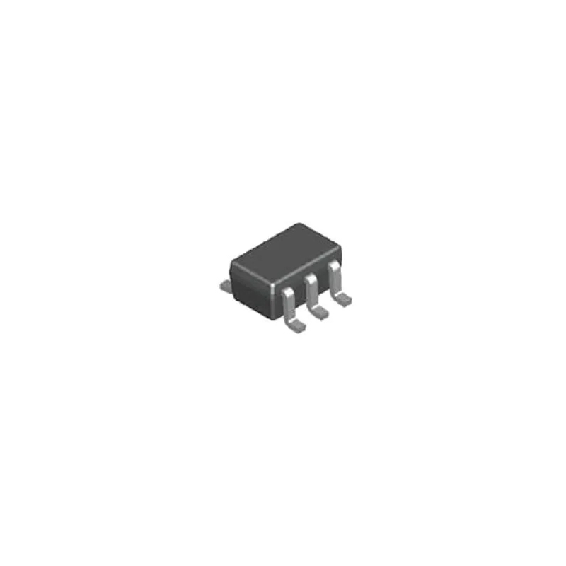
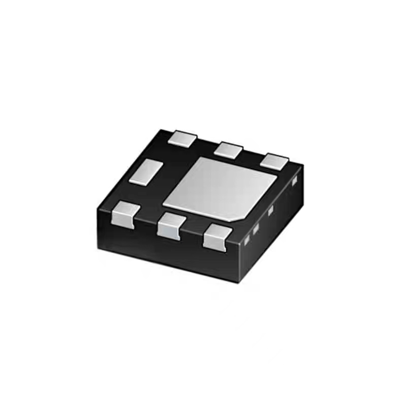
74LVC1G07GW,125
Buffers & Line Drivers 74LVC1G07GW/SOT353/UMT5
品質保證
品質保證
從我們的供應鍊網路採購的所有零件都經過嚴格的進貨檢驗流程。 這種細緻的檢查可確保客戶收到的零件是正品並符合要求的標準。 此外,我們還保存這些檢查的詳細記錄,以確保整個供應鏈的透明度和可追溯性。


認證
我們已成功獲得各項認證標準,並建立了自己的專業檢測實驗室。 這確保了我們向客戶提供的每件產品都符合最高的品質標準。 我們遵守嚴格的測試協議,以保持我們產品的一致性和準確性。 為了確保我們的產品是原裝正品,我們還與信譽良好的第三方檢測機構合作進行嚴格的品質測試。 我們對品質的承諾延伸到滿足行業、法律、監管和 ISO 9001:2015 的要求。
運輸與付款
運輸與付款
關於運送
我們通常會在幾個工作日內通過可靠的運輸公司(例如 FedEx、SF、UPS 或 DHL)運送訂單。 我們還支持其他運輸方式。 如果您想詢問具體的運輸細節或費用,請隨時與我們聯繫。


關於付款
我們接受多種支付方式,包括VISA、MasterCard、銀聯、西聯、PayPal等渠道。
如果您有特定的付款方式或想詢問費率和其他詳細信息,請隨時與我們聯繫。

電匯

Paypal

信用卡

西聯匯款

速匯金
服務與包裝
服務與包裝
About After Sales Service
All Parts Extended Quality Guarantee
自發貨之日起 90 天內發起申請。
與我們的工作人員確認退貨或換貨。
保持貨物收到時的原始狀態。
最後請注意,退貨或換貨的資格取決於對退貨商品實際狀況的評估。 在完成退貨或換貨流程之前,我們將評估收到的貨物。 如果您對退貨或換貨有任何疑問或需要進一步幫助,請隨時通過以下方式聯絡我們: [email protected]
關於包裝
在包裝方面,我們的產品均精心包裝在防靜電袋中,以提供ESD防靜電保護。 外包裝堅固耐用且閉合牢固。 我們支持各種包裝方法,例如捲帶式、切帶式、管式或託盤式。

例子

捲帶式

剪膠帶

管或託盤
74LVC1G07GW,125 數據表
價格 (USD)
| 數量 | 單價 | 總價 |
|---|---|---|
| 10 | $0.056 | $0.56 |
| 100 | $0.046 | $4.60 |
| 300 | $0.040 | $12.00 |
| 3000 | $0.035 | $105.00 |
| 6000 | $0.032 | $192.00 |
| 9000 | $0.030 | $270.00 |
這些價格會受到市場波動的影響,需要提交報價才能取得最新價格。
詳細說明
The 74LVC1G07GW,125 is a versatile single buffer with open-drain output, perfect for use in a variety of electronic applications. Its ability to be driven from both 3.3 V and 5 V devices makes it an ideal choice for mixed voltage environments, offering seamless translation between different voltage levels. Additionally, the Schmitt-trigger action present at all inputs ensures that the circuit remains tolerant of slower input rise and fall times, enhancing its reliability and performance

主要特徵
- Single-element buffer/line driver with open drain non-inverting logic type
- Packaged in 5-TSSOP ReelR Alternate Packaging

規格
以下是所選零件的基本參數,涉及零件的特性及其所屬類別。
| Part Life Cycle Code | Active | Part Package Code | TSSOP |
| Pin Count ! | 5 | Reach Compliance Code | compliant |
| ECCN Code | EAR99 | HTS Code ! | 8542.39.00.01 |
| Family | LVC/LCX/Z | JESD-30 Code | R-PDSO-G5 |
| JESD-609 Code | e3 | Length | 2.05 mm |
| Logic IC Type | BUFFER | Moisture Sensitivity Level | 1 |
| Number of Functions | 1 | Number of Inputs | 1 |
| Number of Terminals | 5 | Operating Temperature-Max | 125 °C |
| Operating Temperature-Min | -40 °C | Output Characteristics | OPEN-DRAIN |
| Package Body Material | PLASTIC/EPOXY | Package Code | TSSOP |
| Package Shape | RECTANGULAR | Package Style | SMALL OUTLINE, THIN PROFILE, SHRINK PITCH |
| Packing Method | TR, 7 INCH | Peak Reflow Temperature (Cel) | 260 |
| Propagation Delay (tpd) | 8.4 ns | Seated Height-Max | 1.1 mm |
| Supply Voltage-Max (Vsup) | 5.5 V | Supply Voltage-Min (Vsup) | 1.65 V |
| Supply Voltage-Nom (Vsup) | 1.8 V | Surface Mount ! | YES |
| Technology | CMOS | Temperature Grade ! | AUTOMOTIVE |
| Terminal Finish | TIN | Terminal Form ! | GULL WING |
| Terminal Pitch ! | 0.65 mm | Terminal Position | DUAL |
| Time@Peak Reflow Temperature-Max (s) | 30 | Width | 1.25 mm |
| Manufacturer | Nexperia | Product Category ! | Buffers & Line Drivers |
| RoHS | Details | Number of Input Lines | 1 Input |
| Number of Output Lines | 1 Output | Polarity | Non-Inverting |
| High Level Output Current ! | - | Low Level Output Current ! | 32 mA |
| Quiescent Current ! | 100 nA | Supply Voltage - Max | 5.5 V |
| Supply Voltage - Min | 1.65 V | Operating Supply Current | 4 uA |
| Minimum Operating Temperature | - 40 C | Maximum Operating Temperature ! | + 125 C |
| Mounting Style | SMD/SMT | Package / Case | TSSOP-5 |
| Brand | Nexperia | Function | Buffer/Driver |
| Height | 1 mm | Input Signal Type | Single-Ended |
| Logic Family | LVC | Logic Type | Buffer |
| Number of Channels | 1 Channel | Operating Supply Voltage ! | 1.65 V to 5.5 V |
| Output Type | Open Drain | Pd - Power Dissipation | 250 mW |
| Product Type ! | Buffers & Line Drivers | Propagation Delay Time | 4.5 ns |
| Factory Pack Quantity | 3000 | Subcategory | Logic ICs |
| Supply Current - Max | 200 uA | Part # Aliases | 935266681125 |
| Unit Weight | 0.000212 oz | Series | 74LVC |
| Product Status | Active | Number of Elements | 1 |
| Number of Bits per Element | 1 | Current - Output High, Low | -, 32mA |
| Voltage - Supply | 1.65V ~ 5.5V | Operating Temperature ! | -40°C ~ 125°C (TA) |
| Mounting Type | Surface Mount | Supplier Device Package | 5-TSSOP |
| Base Product Number | 74LVC1G07 |
數據表 PDF
數據表記錄了器件的特性、絕對最大額定值、應用等,這對於作為器件特定應用的整體指南大有裨益。
常見問題解答
What is 74LVC1G07GW?
The 74LVC1G07GW is a single buffer/driver with open-drain output designed by Nexperia. It is ideal for applications requiring voltage level translation, driving high-capacitance loads, or providing a wired-OR function.
How Does 74LVC1G07GW Work?
The 74LVC1G07GW operates as a single buffer/driver with an open-drain output, enabling it to drive signals to other devices or act as a wired-OR gate. It can be used to level-shift signals between different voltage domains or to drive signals with higher current capabilities.
How Many Pins does 74LVC1G07GW have and What are the Functions of the Pinout Configuration?
The 74LVC1G07GW is housed in a 6-pin TSSOP (Thin Shrink Small Outline Package) package. The pinout configuration includes:
- GND: Ground pin.
- A: Input data pin.
- Y: Open-drain output data pin.
- OE: Output enable input pin.
- VCC: Power supply pin.
- n.c.: Not connected pin.
What are the Pros and Cons of 74LVC1G07GW?
Pros:
- Small Footprint: The 6-pin TSSOP package is space-efficient, suitable for compact designs.
- Open-Drain Output: Provides flexibility in driving signals and implementing wired-OR functions.
- Wide Operating Voltage Range: Supports a wide voltage range for versatile compatibility.
- Low Power Consumption: Operates with low power, suitable for portable devices.
- High-Speed Operation: Capable of high-speed data transmission.
Cons:
- Single Channel: Limited to a single buffer/driver channel, may not be suitable for multi-channel applications.
- Noisy Environment Sensitivity: Open-drain outputs may be more susceptible to noise in certain applications.
Are There Any Equivalents/Alternatives to 74LVC1G07GW for Recommendation?
- The SN74LVC1G07 from Texas Instruments is an equivalent alternative to the 74LVC1G07GW.
- Alternatives to the 74LVC1G07GW include the NC7SZ07 from Fairchild Semiconductor and the TC7SZ07FU from Toshiba.
推薦零件
-
![74AXP1T34GWH]()
Voltage Level Translator 1-CH Unidirectional 5-Pin TSSOP T/R
製造商: Nexperia 包裝/箱: TSSOP-5
4,303 有存貨
貨物週期: 3~7 天
最小訂購量為 1
-
![74LVC1G157GW]()
6,060 有存貨
貨物週期: 3~7 天
最小訂購量為 1
-
![74LVC2G17GM,115]()
5,194 有存貨
貨物週期: 3~7 天
最小訂購量為 1
-
![NPIC6C596ABQX]()
2.3V~5.5V Serial to Serial or Parallel DHVQFN-16-EP(2.5x3.5) Shifting Register ROHS
製造商: NEXPERIA 包裝/箱: QFN16
3,505 有存貨
貨物週期: 3~7 天
最小訂購量為 1
-
![PMEG10030ELP]()
6,454 有存貨
貨物週期: 3~7 天
最小訂購量為 1
-
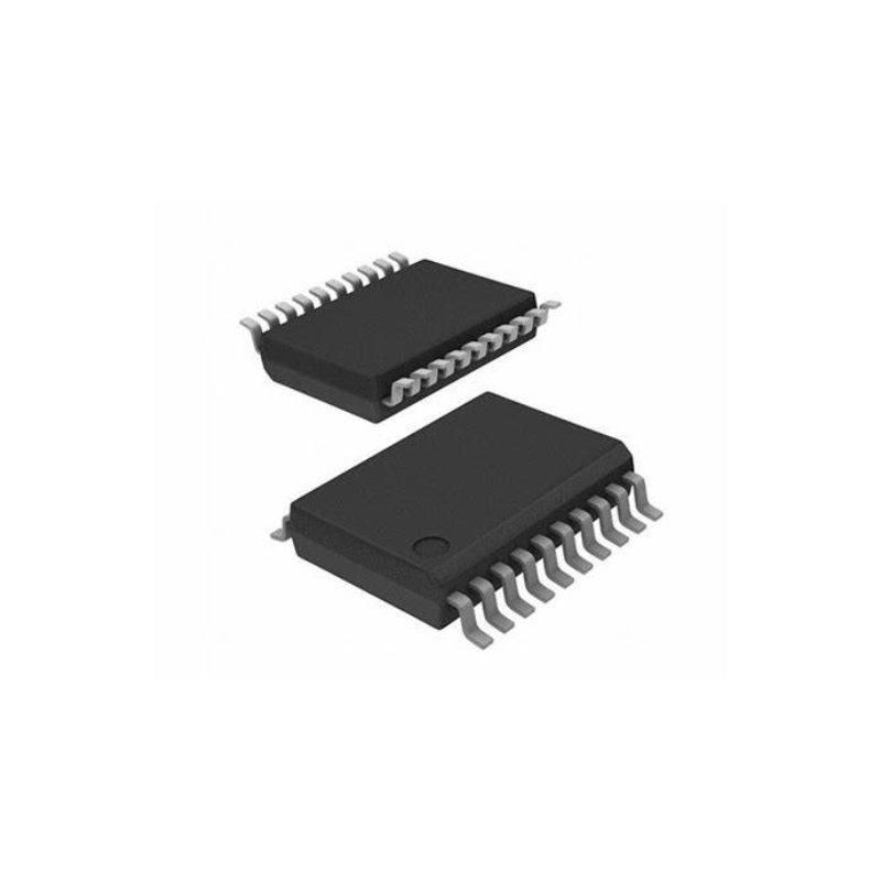
![LSF0108PWJ]()
LSF0108PWJ
$0.202 Translation - Voltage Levels LSF0108PW/SOT360/TSSOP20
製造商: Nexperia 包裝/箱: TSSOP-20
5,039 有存貨
貨物週期: 3~7 天
最小訂購量為 1
-
![NXS0108PWJ]()
Translation - Voltage Levels NXS0108PW/SOT360/TSSOP20
製造商: Nexperia Usa Inc. 包裝/箱: TSSOP-20
8,909 有存貨
貨物週期: 3~7 天
最小訂購量為 1
-
![HEF4015BT,653]()
5,295 有存貨
貨物週期: 3~7 天
最小訂購量為 1
-
![CBT3384PW,118]()
6,239 有存貨
貨物週期: 3~7 天
最小訂購量為 1
-
![CBT3251D,118]()
Encoders, Decoders, Multiplexers & Demultiplexers CBT3251D/SOT109/SO16
製造商: Nexperia 包裝/箱: 16-SO
6,869 有存貨
貨物週期: 3~7 天
最小訂購量為 1
-
![CBT3244APW]()
5,937 有存貨
貨物週期: 3~7 天
最小訂購量為 1